User2User 2024: Meeting future performance demands through packaging: ChipletZ
In this User2User 2024 3DIC session entitled, Meeting future performance demands through packaging, co-presented by Jeff Cain, VP of Engineering at ChipletZ, and Ian Gabbitas, AE Consultant, IC Packaging at Siemens, discuss the advancements and challenges in chiplet technology and packaging solutions. The presenters delve into the specifics of Chipletz’s innovative approaches, including the integration of RDL and embedded components in substrates and how Siemens’ tools aid in managing complex design iterations.
The presentation highlights the importance of these technologies in enhancing performance scaling and addressing power integrity issues in modern electronic designs. It also highlights Siemens’ advanced tools for handling complex via structures and physical reuse in electronic design, emphasizing their importance in managing increasing design complexity.
What is Chipletz Technology, and why is it significant?
While “chiplets” refers to the design approach of disaggregating system-on-chips into multiple dies to address performance scaling and IO bandwidth limitations, “Chipletz” (with a Z) is a startup providing substrate solutions to physically enable chiplet-based architectures. As a substrate vendor, Chipletz aims to make it more viable to integrate heterogeneous chiplets onto a single package substrate, overcoming key implementation challenges.
Chipletz advanced substrate technology facilitates efficient chiplet integration, which is becoming increasingly crucial for AI and high-performance computing applications demanding massive parallelism and bandwidth. By offering an optimized substrate platform, Chipletz complements the chiplet design methodology with a hardware realization path, unlocking the full potential of chiplet-based solutions to meet the insatiable demands for advanced packaging structures and industry collaboration.
Advanced package design techniques
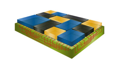
Advanced packaging technologies are enabling the embedding of passive components like capacitors directly into the package core, providing decoupling and filtering capabilities. This is facilitated by innovative feed-through capacitor designs that allow the capacitor to span multiple layers within the substrate. Embedding reduces the overall layer count requirement, leading to better manufacturing yields and lower costs. Furthermore, complex via structures are being employed to improve signal and power integrity. These intricate via arrangements, coupled with the embedded components, result in highly integrated and optimized package designs, pushing the boundaries of performance and miniaturization for cutting-edge electronic systems.
Embedding these caps is a true advantage. We can cut the layer count down drastically because we don’t need a bunch of VDD planes.
Jeff Cain, VP of Engineering, Chipletz
Simplifying and automating complex via creation and placement.
To address the challenges of designing complex via structures in advanced packages, innovative tools have been developed to simplify and automate the entire process. This tool leverages 3D analysis capabilities to validate the integrity and manufacturability of proposed via structures, ensuring reliable signal and power delivery. It automates the tedious tasks of naming and building intricate via structures, dramatically reducing design time. These tools also help designers to easily update or replace via structures as needed. By automating and validating these critical aspects of package design, the tool enables designers to focus on higher-level system optimization while ensuring stringent performance, integrity, and manufacturability requirements are met.

Physical reuse in HBM designs
Efficient physical reuse and management of repeatable circuit blocks like HBM channels in advanced package designs is critical. Instead of manual copy/paste, it provides a hierarchical reuse methodology. Designers can place reusable circuit instances through a GUI, with the tool recording instance locations in a CSV file. Placement can be done by picking XY coordinates, snapping to pins/vias, or selecting pins to specify the reusable circuit, orientation, and mirroring. The CSV file captures all instance data, allowing designers to load it back into the tool to automatically instantiate the reusable circuits across the design. This automated reuse flow streamlines updates to the replicated circuit blocks and simplifies managing physical reuse circuits in the design.
Creating planes and power delivery circuits
Our presenters also provide an automated flow for generating planes, ground planes, and power delivery networks in advanced package designs. This flow offers a layered stack view, allowing designers to select and place planes like power/ground across the entire substrate spanning multiple layers. Selecting a specific net for example, the tool automatically highlights via connection points and generates the corresponding plane while enabling on-the-fly adjustments to clearances. A table displays via/pin counts and connection details per layer as the planes are created. This layer-by-layer approach with visual feedback streamlines the intricate process of implementing robust power distribution networks, saving significant time and effort compared to manual plane creation and stitching to accelerate design time.
Watch this informative 3DIC User2User video recording, now available on demand, to learn more about Chipletz’s innovative 3DIC substrate technology for integrating chiplets into a single package to address power and bandwidth scaling challenges, while highlighting Siemens’ advanced design automation tools – Siemens Xpedition Substrate Integrator (xSI) and Calibre 3DSTACK – that simplify complex via structures and enable efficient physical reuse to manage the growing complexities of cutting-edge electronic systems.
If you missed User2User 2024 or attended the event and want to watch the 3DIC sessions again, the library of videos is now available on-demand here: Click here
To learn more about Siemens EDA 3DIC solutions, visit our 3D IC Homepage