User2User 2024: Silicon photonics to integrate chiplets: Swissbit
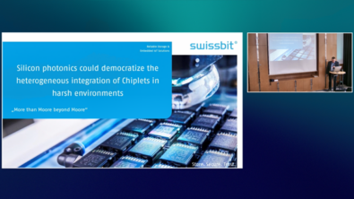
In this User2User 2024 session entitled, Silicon photonics could democratize the heterogeneous integration of Chiplets in harsh environments; Thorsten Grawunder, Sr. System Designer Embedded Solutions at Swissbit Germany AG discusses the integration and advancements in chiplet technology, particularly focusing on the challenges and solutions for heterogeneous integration in harsh environments.
In this presentation Thorsten explores the potential of using chiplets for industrial applications, emphasizing the need for open design architectures to enhance flexibility and cost-effectiveness. The discussion also covers the future prospects of system-on-package designs and the role of photonic integration in overcoming current limitations in data transmission and power distribution.
About Swissbit
Swissbit AG is a manufacturer of storage, security and embedded IoT solutions for demanding applications. Swissbit combines its competencies in storage and embedded IoT technology with advanced packaging know-how enabling its customers to store and protect data in industrial, NetCom, automotive, medical and fiscal applications and across the Internet of Things (IoT). Swissbit produces 2-3 million pieces per month, 70% of which are system-in-package products and operates a 24/7 manufacturing schedule.
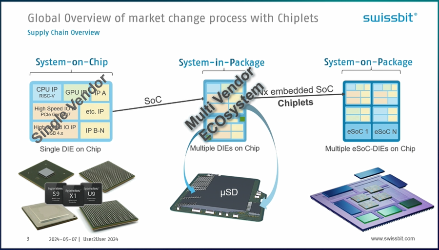
Swissbit’s Chiplet and System Integration
Swissbit focuses on the integration of system on chips with DRAMs or NAND flashes in system-in-package configurations. Their approach to chiplet design differentiates by splitting the system on chip into multiple chiplets for a multi-vendor architecture. Looking to the future, Swissbit projects enhancing their system-on-package designs to more effectively integrate heterogeneous chiplets, further enabling the benefits of chiplet-based system integration.
“The integration of chiplets brings many additional requirements and challenges in manufacturing.
Thorsten Grawunder, Sr. System Designer Embedded Solutions, Swissbit Germany AG
Design and Architectural Innovations
A key area of innovation is the introduction of open Chiplet and assembly design kits that enable flexible, scalable manufacturing approaches. The emphasis is on architectural designs for chiplets from a packaging perspective, rather than traditional front-end chip design flows. However, there are significant challenges in areas like microintegration and advanced packaging that highlight the need for an open source, ecosystem-driven approach to developing these Chiplet design kits. Overcoming manufacturing complexities through innovations in design methodology and architecture will be critical for unleashing the full potential of chiplet-based system integration.
Integration Challenges and Future Directions
As chiplet-based architectures gain traction, especially in demanding applications like automotive, there is a pressing need for comprehensive integration strategies that bake in security and functional safety from the initial design phase. Stringent regulatory compliance mandates are underscoring the importance of incorporating robust security features into chiplet and system designs from the very outset, rather than as an afterthought. In parallel, the semiconductor industry is actively exploring the potential of photonic integration to help overcome interconnect bandwidth limitations between chiplets and enhance overall system performance as more chiplets are integrated together. Tackling challenges spanning security, safety, regulatory aspects as well as leveraging cutting-edge interconnect technologies like photonics will shape the future roadmap for unleashing the true potential of chiplet-based system architectures.
Potential and Challenges of Photonic Integration
Photonic die-to-die interfaces are being explored as a way to potentially replace electrical interfaces between chiplets, with the promise of significantly improving data throughput while reducing power loss from electrical signaling. However, broader adoption hinges on the ongoing development of photonic design kits and standards to facilitate integration across the ecosystem. Looking ahead, the future of highly scalable and efficient chiplet ecosystems may rely on leveraging silicon photonics technology as a key enabler. Overcoming design challenges and establishing an open photonics integration ecosystem will be critical for chiplets to fully deliver on performance, power, and cost benefits compared to traditional monolithic system-on-chip architectures.
Learn more!
Watch this informative User2User video recording, now available on demand, to learn more about how Swissbit is pioneering chiplet and system-on-package solutions that embed security and functional safety from the design phase to meet stringent requirements in harsh industrial and automotive environments. The company champions an open-source approach to chiplet design and assembly methodologies to drive innovation and flexibility across the semiconductor manufacturing ecosystem.
If you missed User2User 2024 or attended the event and want to watch the 3D IC sessions again, the library of videos is now available on-demand here: Click here
To learn more about Siemens EDA 3D IC solutions, visit our 3D IC Homepage