two engineers looking at a PCB design in Xpedition software

Elevating enterprise project success: The power of managed design review workflows in PCB design

A single error in a PCB layout can lead to costly re-spins, significant project delays, and even product failure in the field. Enter managed design review workflows for PCB design.

Cloud-native PCB design: a new era of agility, security, and scale 

In this episode of the Printed Circuit Podcast, guest host Matthew Walsh — stepping in while Steph Chavez attends PCB West — welcomes Adam…

fabricator etching a PCB

Etch effects exposed: discover where your copper really goes

Etching inner layers involves cleaning the copper on both sides of the piece of laminate, applying a photoresist, exposing the photoresist to create the inner layer pattern, developing the resist, etching away the unwanted copper, and removing the etch resist. This process is automated in most shops and the chemistry is automatically monitored. As a result, the accuracy and repeatability is quite good. It is possible to etch inner layer traces using this process to an accuracy of ±0.5 mils. This accuracy control helps keep impedance within the tolerances required for transmission lines.

Fragmented pillars representing fragmented data.

From fragmented to connected: Rethinking the electronics design journey

How digital design threads connect concept, design, and manufacturing to reduce risk, rework, and time to market.

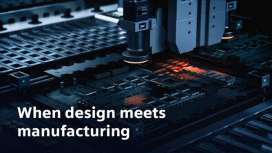
An image of a PCB fabrication process

When design meets manufacturing: Why the digital thread and digital twin are leadership imperatives

When design and manufacturing operate without a cohesive digital twin, the consequences ripple across the enterprise.

An engineer using PartQuest Design Enablement software

Why the engineer’s design journey is becoming the new competitive battleground

Many hardware engineers today navigate an increasingly fragmented digital landscape. The white paper discusses design enablement as a modern solution — one that transforms component manufacturers from passive content providers into active design partners.

Engineers working on PCB designs.

Optimizing multi-domain collaboration: turning engineering complexity into competitive advantage

Multi-domain collaboration is no longer a technical nice-to-have. It is a business imperative.

Icons for PCB components and design processes.

Top 5 benefits of Xpedition Standard

Xpedition Standard brings enterprise-level PCB design power into a flexible, approachable environment that evolves alongside your business.

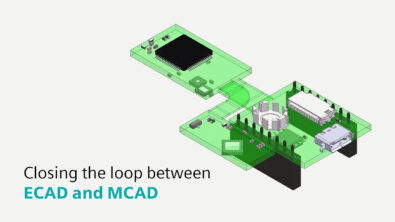
3D view of a rigid-flex pcb design.

Closing the loop between ECAD and MCAD: seamless ECAD-MCAD collaboration through IDX and Xpedition

Unite electronic and mechanical design teams with Xpedition Standard’s built-in ECAD-MCAD collaboration. Discover how the IDX framework enables real-time synchronization, preserves design intent, and eliminates data bottlenecks for faster, error-free PCB development.