PCB design best practices: multi-board PCB design
What is multi-board PCB design?
Multi-board PCB design is the design of multiple printed circuit boards that make up one assembly known as a Sub-system. This Sub-system is part of a System that typically makes up a System of Systems, such as an automobile, an aircraft, etc.
What’s not working?
Today, systems designers mostly rely on desktop drawing programs, spreadsheet editors, and document editors. These outdated processes often lead to manual efforts and a higher risk of human errors. Using a drawing tool and a spreadsheet for systems design just doesn’t cut it anymore. Products are getting more complex and faster, while hardware space is shrinking. It’s a nightmare to define connector pin assignments and verify connectivity, and even with thorough review, errors can slip through the cracks and cause serious financial damage.
When changes happen (and they always do), you have to painstakingly check and double-check every affected connector. It’s not just one level – it’s multiple levels that require manual data management. So every change means checking in two or more places. Without an integrated connection between system design and PCB design, we’re wasting valuable time, making errors left and right, and causing project delays.
Hardware system design is complicated. The current methods we have in place to manage this complexity are reaching their limits. There’s simply not enough time to manually define and handle the intricate designs of modern products. The current methods are time-consuming, error-prone, and require redundant data entry at multiple stages of the design process.
These limitations are costing us time and money in new product design. Errors not only consume resources but also lead to missed opportunities. Just one faulty interconnection can cause delays, expensive resolutions, and even product recalls.
It’s time for a change. We need a better way to manage system design, one that saves time and money, reduces errors, and keeps our projects on track.
What are the roadblocks?
The roadblocks to implementing changes to these legacy processes include:
- Current legacy process is good enough, therefore no need to change
- Internal company culture resistance to change
- Team members work in silos
- No time to acquire additional education/training
- Users not being proficient or experienced with the tools
- Tools are too expensive to set up, implement and maintain
Best practices: multi-board PCB design
The best practices would be to implement model-based systems engineering for cross system optimization regarding size and performance.
As well as you remove siloed engineering teams, the value you would get from these best practices would be system level integration and analysis, A digital twin, tightly integrated collaboration, Cross system optimization removes potential for errors and reduces reschedules, respins and cost.
How it works: multi-board PCB design
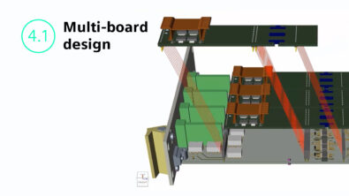
The Xpedition Multi Board System design flow is a fully parallel collaborative design environment where global teams can work on the same design in real time. Systems where multiple boards are interconnected can be created and managed in Xpedition, starting with the logical representation of the design all the way to the physical implementation and layout, including net line connectivity showing between boards and 3D. It supports cable connectivity, definition and optimization, and CAD integration and management through two BOM and manufacturing drawings. It is a single integrated environment that enables multiple board system design including logical design, partitioning and connector and wiring management. Your entire hardware design from multi board electronic system specification to completed PCB’s and cables can be handled within one integrated flow.
Learn more about multi-board PCB design on our website or watch this short video.