PCB design best practices: signal integrity analysis
As a part of pillar three, digital prototype-driven verification, let’s dive into signal integrity analysis.
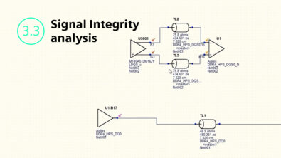
What is signal integrity analysis?
PCB signal integrity is the study of the analog switching behavior of high-speed digital signals. We like to think of digital signals as the square waves we see in logic timing diagrams, but that’s now how they look in real life – they’re far messier, often to the point of being unrecognizable as digital signals. That happens because how we place components and route signals affects how those signals behave, if the devices are fast enough. Bottom line – if it matters how the components get placed and the trace gets routed – you’ve crossed into the realm of requiring signal integrity.
How does someone know they need signal integrity analysis?
When we send a signal out from a driver down a trace towards a receiver, we’d like to think the signal travels to the receiver and simply stops – a nice clean edge. But that’s not how electromagnetic waves work – while they do propagate and eventually settle out, the details matter. We begin to see issues when the ratio of the driver’s edge rate to the trace’s electrical length reaches a critical value. If the driver’s edge rate is slow enough, the signal has plenty of time to propagate and settle down, so the signal’s behavior appears to be the same everywhere on the trace. Think of a long, narrow rectangular pool – if you pour water into one end slowly enough, the water appears to rise evenly all through the pool’s length. However, if you pour a lot of water in all at once, you’ll see a very clear wavefront going out from where your end, sloshing back and forth in the pool until things eventually settle down.
The critical point where you need to start thinking about signal integrity – is when the driver’s edge rate is about 1/6 the electrical length of the net. That lets the signal propagate down to the receiver and back to the driver 3 times during an edge – slow enough, generally, to prevent “sloshing”. If the driver’s edge rate is any faster than that, then we start to see the kinds of effects (reflections, ringing, crosstalk) that require signal integrity analysis to evaluate and mitigate.
That’s a simple overview, of course – as edge rates decrease and data bit rates increase, the physical phenomena that need to be considered become increasingly complicated – and the analysis increasingly sophisticated – to the point where much of the signal integrity simulation that gets run today is performed by dedicated specialists who run signal and power integrity simulations full-time.
What’s not working today?
Most of the signal integrity analysis that gets performed today is run by full-time specialists; they’re dedicated to those tasks. The problem is, there are far too few specialists to service way too many PCBs being designed. With the definition of “high-speed” from, virtually every net on every board these days can be considered “high-speed” – and there’s no way all those nets on all those boards can be analyzed.
To deal with the “SI expert crunch”, most systems companies have adopted two design approaches:
- Pre-route design space exploration (use of signal integrity analysis tools to determine an optimal placement and routing strategy) is only performed where absolutely required. The preferred method is to place and route the design based on guidelines supplied by the component vendors, which assumes that the vendors have, in fact, done those studies and that the board design assumptions they made (stackup, board size, etc.) are applicable to the customer’s intended application. In theory, this approach works fine – but in practice, the “one size fits all” approach to design rules drives up board costs. Additionally, vendor layout rules often get bent or broken and those issues often don’t get caught until a board is in the lab.
- Post-route design verification (simulation of the board as-designed to determine operating design margins) is often minimal or non-existent. The processes most systems companies use for post-layout signal integrity analysis are labor-intensive, and there just isn’t time for that. So – most companies settle for a visual design review, and if post-layout simulation is performed at all, it’s limited to a handful of signals that are meant to cover the extremes – the shortest net, the longest net, and so on. The problem is – layout problems creep in randomly; you can’t rely on being able to pick the signals where problems occur, so this approach lets layout problems slip through to prototype manufacturing. That means problems are discovered and debugged in the lab, and the board must be respun.
What are the roadblocks?
Signal integrity analysis, traditionally, has been a process implemented by (with EDA tools designed for) dedicated specialists. As the technical challenges have become tougher, analysis tools have become more sophisticated and difficult to use. It’s easy to produce results with a simulator – but it’s not always easy to produce results that reflect how a design will really work. Because the state of the art in signal integrity moves so fast, most analysis tools have focused solely on solving the “state of the art” problems, leaving usability as a problem to be addressed later. The problem is – “later” never comes, so the tools become more complex, hard to use and prone to producing erroneous results if not set up by an expert user.
And so – the gulf between what simulation specialists can run and the simulations that need to be run continues to grow. Here again, the “one size fits all” approach is the problem – most EDA tools are developed as though state-of-the-art analysis was the only problem, when in fact, most designs (and potential users) would be better suited by tools that were somewhat less sophisticated but considerably more usable.
Let’s consider an analogy in the automobile industry. If speed were the ONLY thing that mattered, then it would make sense to say that all cars should be Lamborghinis, or an equivalent. But while Lamborghinis are fantastic cars, they’re not very practical for taking the kids to their soccer game, driving in the snow in New York City, or hauling wood home from the lumberyard. One size fits all doesn’t work for automobiles; it’s time we realized that approach doesn’t work for signal and power integrity analysis either.
Because signal integrity is practiced by relatively few people, it is poorly understood by many, with an associated set of myths. To list a few:
- Every simulation should be as accurate as possible: NO simulation is completely accurate, ALL simulations represent a tradeoff between accuracy, analysis speed and the expertise needed to setup and run the analysis. If you want to measure 12 feet of rope, do you use a micrometer? When you’re first roughing out a design, basic simulations work just fine. If you’re designing vias for a PCIe-5 link that will run at 32 GT/s, you don’t need to model them out to 100 GHz. You use the approach – and the level of accuracy, that’s appropriate for the job you’re doing. If you simulate with vastly more accuracy than is really needed, all you’re really doing is slowing your design process.
- You don’t need to understand how things work, because you have a simulator: Simulators augment your understanding of your design and how it works, but they’re not a substitute for structured thought and good engineering judgement. A simulator is a tool, nothing more. It won’t make decisions for you any more than a hammer will frame a wall on its own. Simulators don’t make design decisions – informed engineers do.
- The best simulator for any job is the most accurate one: This is problematic on two levels – first, there’s no proving “most accurate.” That’s a situation-based value judgement at best. Second – you need different capabilities in different situations. When you’re roughing out a design before layout – speed, ease of use and ability to visualize lots of results might be preferable. If you trying to optimize vias for a 224 GT/s link, then that’s where accuracy will be paramount, even if you have to wait a day or more for the results. If you’re trying to verify a board after layout to find potential problems, then automated post-layout extraction, analysis speed and the ability to find a “needle in the haystack” problem are what you will need.
Best practices: signal integrity analysis
The temptation with any simulation tool is to set up the complete problem in a much detail as possible, push the “run” button, then stand back and wait to be amazed. In actual practice, however – that rarely works.
It’s better to be pragmatic – start with an analysis problem that is as simple as possible – one where you literally know what the answer is beforehand – to be sure that the setup and the simulator are working properly. That’s not glamorous, but it is practical – simulators are complex, with lots of settings and options, some of which can cause erroneous results. Start with something that you know works, then add modeling and analytical complexity in stages, testing and verifying as you go. You’re far more likely to end up with a simulation result that you’re willing to bet a design decision on.
Another advantage of building an analysis in stages is that you can gauge the impact different structures and physical effects have on design margin, so you know what problems you really need to focus on. If you analyze a serial link with skin effect only and get an eye height of 60mV, then add surface roughness and get 45mV, then add crosstalk and get 40mV … all against an eye height requirement of 35mV … then it’s probably time to start thinking about your stackup, what layers you’re routing you signals on, and whether it’s time to investigate better copper treatments.
Eric Bogatin has a great saying – the accuracy you need in your analysis goes up as your design margins go down. Knowing what physical effects you’re modeling and how much margin is being lost to each effect is key.
How it works: signal integrity analysis
There are two basic kinds of signal integrity analysis – pre-layout design space exploration, which seeks to derive rules needed to place and route the board, and post-layout verification, which seeks to simulate the board as-designed to ensure it is OK to fabricate.
Pre-layout design space exploration is performed from a schematic that lets the user place transmission lines (representing traces), vias, connectors and passive/active components. Following best practices, you start with a very simple topology and add detail in controlled stages, simulating as you go. Pre-layout analysis explores design and topology variations to derive a set of rules that will drive placement and routing to ensure adequate design margin.
Post-layout verification is important because not everything in PCB layout goes according to plan. Rules get broken, mistakes get made – and finding them with prototypes in the lab is time-consuming and expensive.
HyperLynx uses a strategy called Progressive Verification, with the goal of finding as many problems as possible, as quickly as possible, with as little effort as possible. Progressive Verification occurs in 3 main stages – Design Rule Checking, Standards-based Analysis and Vendor-based Analysis.
Design Rule Checking takes the place of traditional visual design inspection – a distinct improvement, since computers don’t get tired or bored. HyperLynx DRC has a rich set of expert-based rules than can be configured to automatically inspect designs for common electrical problems. For example, HyperLynx DRC can check an entire design database to find areas where traces cross over plane splits in a manner of seconds. Finding problems like this using visual inspection is tiring and error prone; finding problems like this with modeling and simulation is surprisingly time-consuming and difficult. Keeping with the Progressive Verification strategy of taking problems as quickly as possible, HyperLynx DRC lets users find and resolve many different types of problems quickly.
Next, Standards-based Analysis focuses on the PCB interconnect (the part of the system that system designers actually design) and ensures it meets an requirements associated with the standard. In the case of SerDes-based serial links, the different Protocol Standards define requirements for the channel itself, independent of the transmitter and receiver at either end of the channel. The transmitter and receiver (and their simulation models, and the simulation process used to predict their behavior) will change from vendor to vendor and device, but the requirements for the channel itself (and the process used to assess compliance with those requirements) will not. That means the Compliance Analysis process is well-defined and can be automated – which is exactly what HyperLynx does. Assessing interconnect for compliance is the logical next step in validating an interface, because it’s not vendor-model dependent. It’s faster, it’s easier and it gives designers a good understanding of how their interconnect performs, before taking the final step of analyzing the interconnect with the actual silicon devices driving and receiving signals from it.
The final step in Progressive Verification is simulating the interconnect as-designed, together with the actual silicon devices and their associated settings (drive strength, receiver termination, equalization, etc.). This requires accurate, complete models from the device vendors. Availability of these models can be problematic – but that’s another reason why Standards-based Analysis is so useful – it works even when vendor models aren’t available. When available, vendor models provide the most accurate simulation results possible – but they also require the highest level of expertise to obtain, validate and use.
Bottom line – simulation tools are awesome, but they’re not magic. They’re like any other powerful, sophisticated tool – they require a strong understanding of the problem to be solved and how to apply the tools to the problem – to achieve the desired result.
For more information on signal integrity analysis visit our website or watch this video:


