PCB design best practices pillar 3: digital prototype-driven verification
Today I will outline our third pillar of PCB design best practices, digital prototype-driven verification.
When it comes to digital prototype-driven verification, what really matters is eliminating physical prototyping with automated design reviews, evaluating multidiscipline tradeoffs, empowering design engineers with accessible technologies that reduce dependency on experts, and co-optimization of silicone package and board systems.
When we think about digital prototype driven verification, I see two typical problems often taking place today:
- Analysis is run too late. Respins tend to be normalized because the team has already accounted for two or three respins in the schedule. Worse, analysis is not done at all, and is often pushed off because time in the project schedule becomes a major concern. Knowing there is a risk, the decision is made to take short cuts in the process to get the design out to fabrication as soon as possible since analysis can always be run on the next revision.
- The domain specialist or subject matter expert tends to be working in a silo or is too far downstream in the process, causing late edits or modification to the design that potentially can negatively impact schedule.
A shift-left methodology
After several decades of designing boards, when it comes to analysis, I strongly feel this is a stage in the design process that needs to be done. You shouldn’t skip this step merely to reduce the project schedule, because it will bite you in the end, especially when designing complex PCBs. Left shifting steps, to include analysis, within the design process as much as possible is the best approach. This has the highest potential for reducing project schedule and cost. Analysis such as thermal, signal integrity, power integrity, electromagnetic compliance (EMC), analog mix signal (AMS), and design for manufacturing (DFM), should be done sooner (upstream) in the project, that way you’re catching and eliminating errors as the design progresses, comes to completion, and before you’re ready to release to fabrication and assembly. This way you’re designing quality into your design. You’re not simply checking for quality after the fact. By then, its tool late and becomes more expensive to make last minute edits or modifications.
Now when it comes to the domain specialist, you want to optimize multi domain integration so that way your specialist isn’t isolated or becomes an afterthought within the design process. You want to use the domain specialist earlier or in parallel in the process rather than later downstream.
The value of shifting left
Of course, you will have reduced design cycle times, which translates to reduced cost. You’ll remove potential for errors, that potentially present themselves downstream. When you finally get your design into the lab and bringing the board up for the first time, there is less of a chance you’ll run into issues because you designed it correct by construction. Then, when you get into testing such as EMI, you’re not just hoping if the board assembly is going to pass. You’ll take comfort in knowing the potential for success is higher because you ran the analysis up front (upstream).
Within this third pillar there are several PCB design best practices to highlight:
Schematic analysis and verification
Verifying the schematic means fully inspecting all of the net connections in a schematic. In Xpedition this is done by using an extensive component library of intelligent models, saving design teams hundreds of hours of manual efforts and visual inspection and lab debug time, leading to reduced project schedules and cost. This analysis can validate and verify signals across multiple boards in a system. This is not limited to net connections only. We’re also addressing the validation of the actual electrical circuitry in the schematic against the manufacture’s datasheet.
Signal integrity (SI) and EMC analysis
Running simulation of critical signals on a board can save time later on in the design cycle. In the Xpedition flow, analysis can be done early on, even while teammates are finishing the work on other parts of the design. Simulating early allows teams to build constraints for critical nets so that issues can be avoided.
Power integrity analysis
Once a PCB has defined power planes and ICs have been placed and broken out, it’s a good idea to run a DC drop analysis. Doing this earlier in the design process helps users verify that the power delivery is adequate and that issues like fan out vias perforating the power planes have been avoided.
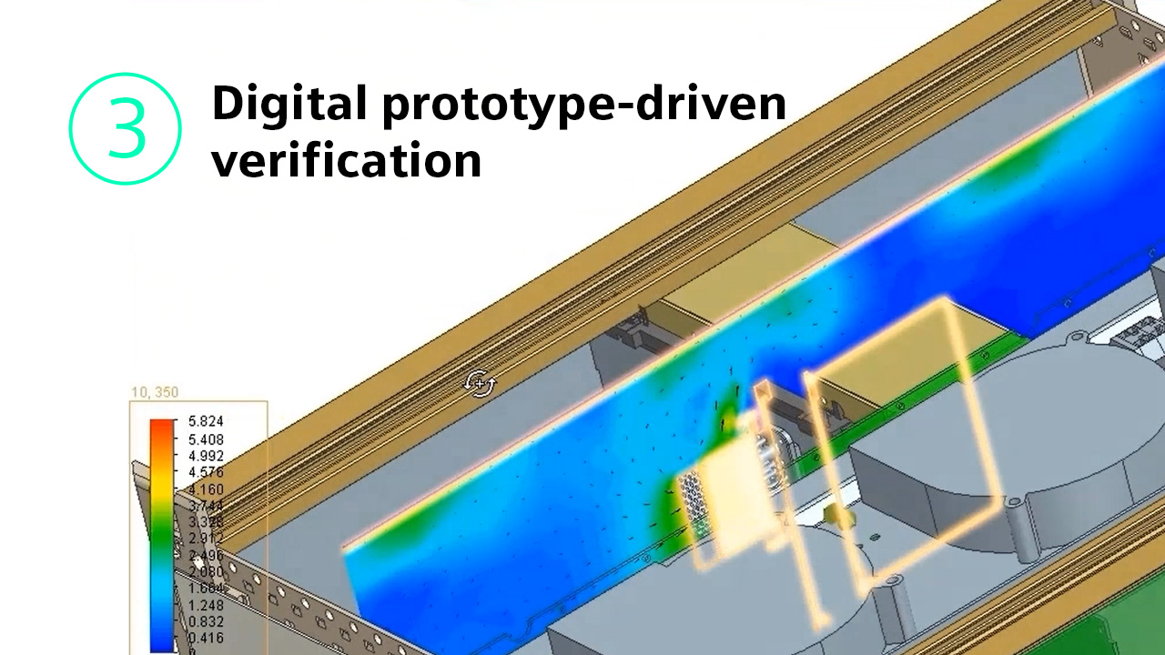
Thermal analysis
Exploring the thermal characteristics of the design can be done as soon as board 3D geometry is created, not necessarily when the design is complete. Thermally relevant information such as fan velocity, if the system has a fan, and heat sinks are considered. Running the simulation of a board within the chassis of the product makes sure that the users get the most realistic results from the simulation run. Several different types of data can be extracted from analyzing the digital prototype. For instance, temperature distribution of the electrical and mechanical components, air velocity within the design, and even data about the temperature change over time can be captured, make it easy to optimize the thermal performance of the end product.
Manufacturability verification
Catching potential assembly and manufacturability issues early in the design process is essential to minimizing design respins. With Xpedition, DFM analysis can be run from within a design layout. Users can fine tune constraint sets to meet their needs. They also control which checks are run at each stage of the layout. Viewing the results of the DFM check is the same as checking the results of the DRC in the tool and since the results are shown in layout issues can quickly be addressed by cross probing to the problem area of the board.
Digital prototype-driven verification
In conclusion, left shifting analysis will allow you to build quality into your design. Not simply check for quality after the fact. It will help you reduce design cycle times and cost.
As we continue along in this series we will zero in on each best practice within this pillar and provide examples of how to implement them, address challenges and overcome roadblocks.
Thanks for following along and make sure to check out the full video on digital prototype-driven verification here.