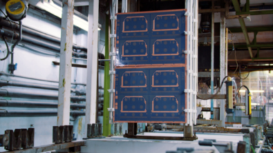
PCB routing: art + automation
PCB routing is one of the most enjoyable parts of PCB design, but also the most time consuming. It may take only a week to layout your board, but it could take you three months to route it unless you have the appropriate automation tools. PCB routing technology is more advanced than in years past, and yet, you can still be very creative and make a beautiful design.
It makes sense to take advantage of the tools that are available to you when routing your PCB to speed up the design process, because today speed and quality are everything. Doing things 100% manually doesn’t cut it anymore. You must be interactive about your PCB routing – doing a little manual combined with automation, especially when working on high speed or high-power designs.
We’ve come a long way from basic PCB routers. Today we’ve got some incredible tools that enable you to leverage PCB routing either in a manual or semi-automatic form. New PCB routing technologies can provide you with a good idea of where your congestion is, and answer questions like:
- Does the current PCB Stackup have enough layers to route the design?
- Will the design need blind and buried vias?
- Does the placement allow for my high-speed routing constraints?
Xpedition has incredible PCB routing functionality!
To start the overall PCB design process…
Good placement leads to good PCB routing
Even before you get to the PCB routing, you have tools today that can optimize your pin package out of the IO. You can drive a much better route based on optimizing the pins of an FPGA or swapping the gates of your devices. This isn’t new technology, but the way it gets done has become much more effective.
A good placement will ensure success when PCB routing; a bad placement, will set yourself up for failure, especially when it comes time to simulate your design. And just like PCB routing, there are tools to use to automate placement. An example would be groups.
With groups you can actually go into an existing layout, pull a whole group of components out and place it in a new design. And the tools have the ability now to not only place this block of data, but you can also keep it in this block and put multiple groups out into the layout phase or into the environment on the board.
The groups are smart enough to know the area from a single side that they’re going to require to be placed on the board. So, you don’t have to drop it all the way down to the to the component level, you can establish these blocks, and then move them around and see the conductivity — heavier lines mean more connections, lighter lines mean less.
Levels of hierarchy
You can have groups within groups, and you can have rules for each one of these groups, where I could say, this lower-level group, which is all the passives, I don’t even want those on the same side as my active devices, and I can set that up within this “properties” menu. So, when I place these groups, the actual devices go to the appropriate level. Maybe I’ve got a huge BGA with a bunch of decoupling and terminating resistors, and they’ll get smacked right onto the backside of the board with me without me even worrying about it.
When you create groups in the Xpedition environment, you can also add mounting holes to that group, you can add seed vias, you can add planes; it can have almost any entity that you want, you just have to make sure it’s a part of that group and then it can be moved anywhere in the board, even off the board so I can see what’s going on. But now back to our primary topic!
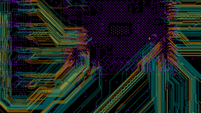
PCB sketch routing and sketch planning
PCB sketch routing and planning provides a set of highly automated routing functions featuring intuitive user control, high quality, and exceptional performance. These automated tools make it look like a human designed the routes, with the ability to autoroute it, delete it, and do it again until you get it the way you like it.
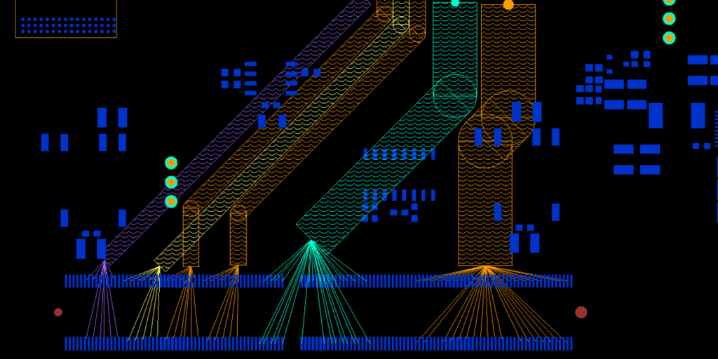
Hug routing
How many times have you routed a bunch of stuff and then realized that there is one net line that wiggles between all those things. In the past, we would’ve had to rip all that up to get that one net line in again. This is where the hug router comes in to play. The hug router is for when you’ve got to use brute force to get that last net in.
The hug router lets us take that one net or two nets that didn’t go in there and we’ll select it and hit the hug route button. It’ll push, shove, and squeak its way in there to make the connection. So, it takes everything we just did in minutes with the sketch router and pushes it out of the way as it squeaks this last net in, and I love the fact that it’ll get that last net connected without you having to take anything apart.
Plow routing
For the Artist in you and for those last stubborn nets Xpedition Layout has few other Routing options that can deliver a solution specific to the types of routing required. The Real Trace Delayed/Dynamic plow functions for manual routing guides the user through already routed areas with visual aid (Green or Red) so you can understand if the path you’re on will work with highly intelligent push and shove capabilities.
This is highly effective in situations that inevitably come up on those last few nets that need to be routed. Last but not in the least, in the case of Analog / RF traces the Hockey Stick or Segment routing provides the user with total control over the exact path you need to go to meet your unique signal requirements.
Learn more about design automation
PCB routing and placement are just two elements of PCB design automation. To dive deeper into this topic listen to our podcast: Design automation best practices or read our design automation best practices blog.