Visit Siemens at PCB West 2023
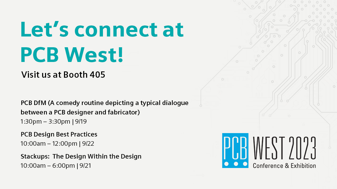
Stop by and see us in booth 405 at the annual PCB West show in Santa Clara, CA on September 19-22, 2023. We will be showcasing Xpedition, HyperLynx and Valor tools through live theater presentations and a dedicated demo station with live product demos.
We also have three presentations being delivered at the conference.
PCB DfM ( A Comedy Route Depicting a Typical Dialogue between a PCB Designer and Fabricator)
Tuesday, September 19th | 1:30pm – 3:30pm


Stephen Chavez | Siemens
Gerry Partida | Summit Interconnect
PCB designers just don’t simply connect the dots or push the magic button, as some may suggest. They design complex PCBs that contain physical packages smaller than ever before while addressing electrical, mechanical, and thermal variables and cost. Success in PCB design means knowing and understanding what you are doing and how the decisions you make and implement upstream have downstream ramifications.
There are key factors in achieving success in PCB design. In this presentation, the speakers focus on the relationship between design and fabrication. We’ll discuss industry best practices within the design to fabrication process, along with the pros and cons that affect ROI when best practice recipes are implemented and when they are not implemented (the cost of doing nothing).
With today’s EDA tools, and eagerness of suppliers offering their technical support, the potential for success is higher than ever. This collaborative approach makes a positive difference in getting it right the first time, reducing respins (cost), increasing yields, and ultimately getting to market faster.
What you will learn:
- Increase productivity and proficiency in PCB design to fab
- Capitalize on existing industry best practices of DfM and manufacturing outputs
- How you can reduce cost
- A short comedy scenario depicting the dialogue between a principal PCB designer and a fabricator
Stackups: The Design Within the Design
Thursday, September 21st | 10:00am – 6:00pm

Bill Hargin | Z-zero
This workshop will guide design teams through the process of evaluating and selecting the right laminate for a design, creating PCB stackups that meet the requirements of complex, multilayer boards that work right the first time, within budget, and with reproducible results across multiple fabricators. The course will go into detail on tradeoffs between loss and cost, including dielectric loss, resistive loss, surface roughness, as well as glass-weave skew. After attending this course, students will be knowledgeable of PCB laminate tradeoffs, the laminate-materials market, and the process of troubleshooting problematic stackup designs. Attendees will also be exposed to cost-effective strategies for controlling loss and glass-weave skew.
PCB Design Best Practices
Friday, September 22rd | 10:00am – 12:00pm
Stephen Chavez | Siemens
PCB designers today must take advantage of the automation and horsepower in our respective EDA tools. We just don’t simply “connect the dots” or “push the magic button,” as some suggest. We design complex PCBs that contain physical packages smaller than ever, but we are also addressing electrical, mechanical, and thermal variables in a much higher level of complexity due to today’s industry evolution, not to mention the need to design it faster while cutting costs and resources. We are designing PCBs that contain signal speeds and edge rates faster than ever. As if the electrical and mechanical design complexity of a PCB weren’t enough of a challenge, add in manufacturing and producibility complexities. All this makes designing entire complex systems a true challenge indeed. Simply put, success in PCB design means knowing and understanding what you are doing and how the decisions you make and implement upstream impact downstream ramifications.
With today’s EDA tools, harnessing the horsepower and capitalizing on their full capability, when possible, can be a huge difference in getting it right the first time, reducing respins (cost), increasing yields, and ultimately getting to market faster.
This session focuses on how to harness the horsepower of your respective EDA tool, optimize your internal processes, and share both good and not so good experiences in PCB design. We will discuss industry best practices within the design process, along with the pros and cons that affect ROI when best practice recipes are implemented and when they are not implemented (the cost of doing nothing).
What you will learn:
- Increase productivity and proficiency with current/future EDA software (automation)
- How to capitalize on existing known good hardware by taking advantage of IP reuse
- Benefits of implementing best practices and the cost of doing nothing (remaining status quo)


