PCB design best practices: manufacturability verification or design for manufacturing analysis
What is design for manufacturing analysis?
Design for manufacturing (DFM) analysis is manufacturability verification within the design process. It incorporates manufacturing constraints/guidelines that are used to check a design for potential downstream manufacturing issues upstream in the overall process to enable the highest potential for success in manufacturing regarding efficiency and optimization within the manufacturing flow.
By collaborating with the DFM experts in your manufacturing supply chain, you can shift left the manufacturing-process-constraint rules to your design and NPI operations. By using the same rules and even the same settings to simulate how your suppliers will review your design, you will minimize callbacks and engineering-change requests, also known as Technical Queries (TQs) from your manufacturers, reducing your New Product Introduction (NPI) cycle time and cost.
What’s not working today?
Designing today’s complex and challenging PCB designs requires multidiscipline and multidomain integration and collaboration. This includes manufacturing! In the legacy (outdated) approach to PCB design, a DFM analysis is an afterthought in engineering, and, in many cases, a DFM analysis is step in the design process that is skipped to save a few bucks in the project budget, or to cut a few days off the project schedule. Worse, DFM is not even a thought at all.
This legacy approach of DFM analysis does not meet today’s design-manufacturing collaboration needs, which ensures an efficient and optimized transition from engineering to manufacturing that enables downstream success. The days are long gone when we could get away with designing complex PCBs without running a DFM analysis. In today’s competitive market, most can no longer afford to design complex PCBs without running a DFM analysis, and then toss our design over the wall to manufacturing in hopes the design can be manufactured with little to no issues with the goal of the highest yield and lowest cost.
Manual tasks within the legacy approach of completing a DFM analysis has the potential for human error(s) to be missed or incorporated in the design. Utilizing engineering tools with limited or no DFM capabilities combined with manual DFM tasks are proven to lead to a high potential for issues in manufacturing, and ultimately leading to unnecessary redo’s and or respins.
What are the roadblocks?
Like any other engineering step, there are several roadblocks that stand in the way of implementing the recommended best practices. Project demands, which include budgets, schedules, and limited resources are a common roadblock. Another roadblock is not having a standard design process in place that includes DFM analysis.
For many, a running a DFM analysis is non-existent step in the design process. This potentially leads to lacking the specific domain/discipline specialist or skillset within the design team, and or working in silos in a non-optimized and inefficient process flow. This this leads to a high potential of skipped/missed steps in the attempt to shorten the project schedule and reduce the project budget. It also increased the potential for having multidiscipline and multidomain integration issues, and repeated mistakes carried over from one project design to another. All leading to un-necessary respins.
Another common roadblock is internal company culture. In this roadblock, I’ll address specifically two items here:
- engineering teams not having access to adequate analysis/simulation tools that are more than capable of meeting today’s challenging complex PCB design needs or not having the necessary expertise/skillset.
- Having those specific team members who have an outdated mindset approach, and that are not open to adapt/evolve with today’s industry’s best practices to meet tomorrow’s designs today. Sadly, having an outdated mindset approach in the attempt of meeting today’s challenging complex designs, along with reduced resources, shortened project schedules, and reduced budgets has a high potential of severely hindering a company’s competitiveness in today’s market.
Best practices: design for manufacturing analysis
The best practice is to include a DFM analysis within in your design process. Utilizing an industry DFM tool such as Valor NPI provides solutions that optimize PCB design/manufacturing with a complete digital-twin flow. Valor assures manufacturability, while the process tools suite helps you create complete manufacturing data. Manufacturing solutions ensure an efficient shop floor and ‘first-time-right’ electronics production. Accelerate the design-to-manufacturing handoff process by connecting designers directly with manufacturers. Run PCB DFM analysis using the updated constraints for a specific manufacturer during the early stages of the design process, reducing design iterations, costs and time-to-market.
How it works: design for manufacturing analysis
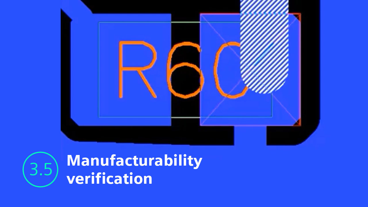
Addressing manufacturing issues early in the design process is crucial for minimizing costly design respins. This is where Xpedition comes into play, offering the capability to perform Design for Manufacturing (DFM) analysis directly within your design layout. You have complete control, determining which checks to conduct at each stage and customizing constraint sets to align with your specific requirements.
With the implementation of Valor NPI DFM analysis technology, Xpedition provides over 1,000 pre-installed checks, ensuring comprehensive coverage from all perspectives. The results are conveniently displayed within your layout, similar to a Design Rule Check (DRC). This means you can easily investigate any problematic areas on your board and promptly address any concerns.
The remarkable aspect of Valor NPI DFM analysis technology is that it enables you to identify and resolve potential manufacturing bottlenecks without the need to leave Xpedition or interrupt your PCB design process. DFM checks can be performed at any point, from component placement to release-to-manufacturing, and the automated DFM reports streamline design reviews, saving you valuable time.
Think of it as having a manufacturing process expert at your disposal, providing valuable insights right from the beginning of the new product design flow.
To learn more about design for manufacturing check out our website or watch this short video:


