Context-Aware Latch-up Checking
By Matthew Hogan, Mentor Graphics
Latch-up detection is challenging. Learn how automated LUP checks help you find and eliminate LUP conditions.

Latch-up in CMOS circuits is a long-studied and troubling phenomenon that often leads to chip failure through the inadvertent creation of parasitic PNP and NPN junctions being driven (turned on/forward-biased). Typically, an unintended thyristor or silicon-controlled rectifier (SCR) is formed and then triggered to generate a low-resistance parasitic path. Latch-up presents itself as a temporary condition that may be resolved by power cycling, but it may also cause fatal chip failure or permanent damage.
Recognizing unintentional failure mechanisms present in an integrated circuit (IC) is a constant and often difficult task for design teams. Increases in design complexity, larger pin counts, more power domains, and the ever-changing landscape of what process node and which foundry will host your next design all contribute to the challenge. Additionally, many of the geometric design rule checks (DRC) traditionally employed for latch-up detection lack the context awareness that modern reliability verification tools can provide. However, getting it right, particularly when you are trying to find and eliminate latch-up in your designs, is of critical importance.
Although no design team enjoys further complicating design and verification flows by adding additional checks, a fully automated latch-up rule check is highly desirable, particularly when multiple power domains are involved. Just as voltage-aware DRC checking [1][2] has provided a significant improvement in the accuracy and control of interconnect spacing for reliability and the avoidance of time-dependent dielectric breakdown (TDDB), context-aware latch-up verification offers similar advantages and opportunities to automate these challenging design interactions.
When considering the impact of latch-up on a layout, understanding both the unintentional devices within your design and how the layout impacts critical distances of specific latch-up susceptible structures is critical. For example, to be able to adjust the layout to prevent latch-up, designers must recognize where unfavorable conditions may lead to unintended parasitic devices formation in the PNP or NPN junctions as current is injected. Figure 1 shows how lateral separation can be used to protect against latch-up formation.
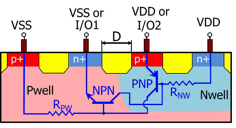
Figure 1 – Latch-up prevention with lateral separation [3]
Impact of voltages and devices
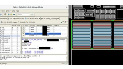
While understanding the distances and physical layout within the design is essential, consideration must also be given to the voltages being used. As with voltage-aware DRC, the voltages being analyzed for potential latch-up conditions have a significant impact on the spacing rules that must be applied. The interaction of these voltages can greatly influence the location of susceptible regions in the design, as well as the location and degree of change necessary to avoid this susceptibility (Figure 2).
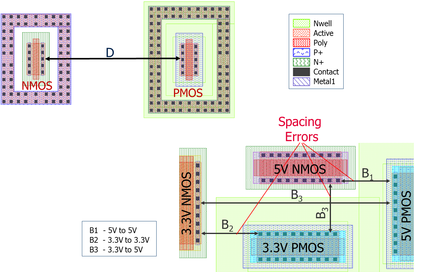
Figure 2 – Accurate latch-up checks require voltage awareness [3]
While a single simple spacing rule may be all that is required with just a few voltages, the complexity of the protection needed increases as more power domains are included. How these domains switch, with different parts of the design being active at different times, adds to this complexity. The ability to leverage the power intent of your design, particularly through descriptions created using the Unified Power Format (UPF), enables a state-driven approach to determine what voltages are present in any given state.
What CMOS technology are you using: Bulk, FD-SOI or Both?
While much of the literature on latch-up assumes that the implementation technology impacted by latch-up is entirely bulk CMOS, and that fully-depleted silicon-on-insulator (FD-SOI) is immune, there are hybrid technologies that leverage characteristics of both FD-SOI and bulk CMOS. One such technology that comes to mind is the ultra-thin body and box (UTBB) FD-SOI process used by ST Microelectronics [4]. UTBB leverages the benefits of a FD-SOI process for the design logic, while taking advantage of a “hybrid” bulk CMOS for electrostatic discharge (ESD) and IO devices. For ESD protection, the ESD device in thin silicon film is two times less robust than the bulk CMOS device (due to the smaller thickness of the Si film for power dissipation). Leveraging an open box structure to access hybrid bulk CMOS configurations to build ESD power devices provides benefits for device robustness. In doing so, however, verification needs to consider possible sources of susceptibility to latch-up in areas of the design with hybrid bulk CMOS IO devices and ESD structures.
Conclusion
While traditional DRC has contributed to a valuable verification methodology for latch-up, it lacks the fidelity and context to fully identify the latch-up susceptible regions in your design. Learning and applying the latest reliability analysis techniques to solve these often intricate and complex verification requirements for latch-up detection, while also developing process improvements to avoid susceptible configurations in future designs, is critical from a best practices perspective.
To assist designers looking to integrate this technology into their design and verification flows, the ESD Association (full disclosure: I am a volunteer and serve on the Board of Directors) has extended its educational offerings in the area of latch-up detection to include these types of complex verification. A new course, DD382: Electronic Design Automation (EDA) Solutions for Latch-up [5], reviews a typical latch-up prevention flow, and delves into details necessary for improvement.
The continued evolution of your organization’s reliability verification checks and best practices, along with the evaluation and adoption of best practices from the industry as a whole, should not only be an aspiration, but a measurable goal to keep your design flows current. Incorporating new learnings into existing flows helps improve both their robustness and relevance for today’s complex designs, and leverages efficiencies learned in the development of new solutions. Latch-up, like many design flow challenges, provides significant opportunities for process improvement and flow automation in the ongoing effort to implement robust and repeatable verification solutions.
References
[1] Medhat, Dina. “Automated Solution for Voltage-Aware DRC,” EETimes SOC DesignLIne, December 23, 2015.
[2] Hogan, Matthew, et al. “Using Static Voltage Analysis and Voltage-Aware DRC to Identify EOS and Oxide Breakdown Reliability Issues.” EOS/ESD Association Symposium, 2013.
[3] Khazinsky, Michael. “Latch-up Verification / Rule Checking Throughout Circuit Design Flow.” Mentor Graphics User2User, 2016.
[4] Galy, Philippe. “ESD challenges for FDSOI UTBB advanced CMOS technologies.” International Electrostatic Discharge Workshop, 2014.
[5] EOS/ESD Association Symposium Tutorials, EOS/ESD Association Symposium, 2016.
Author
Matthew Hogan is a Product Marketing Manager for Calibre Design Solutions at Mentor Graphics, with over 15 years of design and field experience.

Liked this article? Then try this –
Video: How to Check for ESD Protection Using Calibre PERC High Level Checks
This article was originally published on www.semimd.com