What’s all the fuss about shift left?
By Michael White and David Abercrombie
In recent months, it seems as though everyone’s been talking about shift left as a way to improve productivity in integrated circuit (IC) design flows. What, exactly, is shift left? How is it any different from any other productivity initiative we’ve heard about (or tried) over the years?
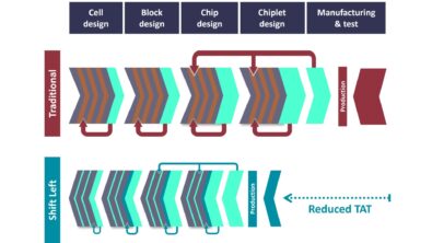
At first glance, shift left may seem like another in a long line of strategies and tactics integrated circuit (IC) design companies have adopted over the years to try to streamline and optimize their design and implementation flows. And that’s one way of looking at it. The semiconductor industry depends on constant innovation and improvement to maintain the steady growth in IC design complexity and size while ensuring their products can still be manufactured. A shift left strategy is certainly part of that trend. At the same time, it’s quite a bit different.
A shift left strategy brings new tools, techniques, and functionality that enable design teams to bring a new focus and new capabilities to design-stage verification. Rather than the limited verification functionality provided by custom design and place and route (P&R) tools, a shift left implementation gives designers and P&R engineers access to the foundry-preferred, full-featured design verification and optimization functionality. At the same time, it concentrates design-stage verification into a targeted and selective set of checks that helps design teams find and correct key systemic and critical errors that, if allowed to slip through the design or implementation stage, will lead to multiple time-consuming verification iterations during signoff. Innovative verification functionality, such as early short isolation, symmetry verification, gray-boxing of missing or incomplete components, and automated waiving of known errors, further helps by eliminating time that would be spent debugging errors that are irrelevant to design-stage verification.
But designers and P&R engineers aren’t physical verification engineers. So shift left doesn’t just throw these new verification processes at them and hope for the best. Additional optimization comes in the form of automated processes and user-friendly, intelligent tools and interfaces that simplify, speed up, and optimize this new functionality. Automated run invocation provides a user-friendly environment that simplifies and speeds up setup, while minimizing, grouping, and visualizing error results and providing results color mapping help designers and engineers quickly identify root cause(s). Automated design for manufacturing (DFM) optimizations help reduce voltage (IR) drop and electromigration (EM) issues while preparing designs for physical verification, without consuming busy (and expensive) P&R licenses. Automated back-annotation ensures layout changes are integrated into the design database for later design flow stages. Tight interfaces between design-stage verification tools and custom design and P&R tools provide design companies with the flexibility to create a mix of best-in-class tools and processes that maximize both productivity and quality of results across the design flow, while ensuring designers and engineers can continue to work as usual in their familiar tool environment.
Perhaps the best news is that shift left itself is an evolving process. Machine learning (ML) and other artificial intelligence (AI) techniques is being used to help automate and refine design-stage layout analysis by identifying new and additional layout issues that are best addressed during design and implementation, as well as locate configurations of results across separate checks that can act as signals to help identify the optimal correction techniques. Intelligent resource forecasting also uses ML to support efficient resource use and provide the fastest turnaround times. Enabling shift left tools with the ability to run using onsite resources or the cloud provides companies with the flexibility to respond to business needs and changing priorities quickly and efficiently.
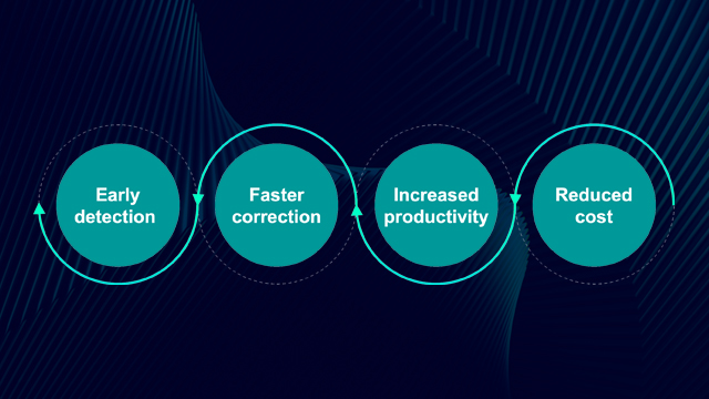
By understanding and applying best practices for the use of these tools, and taking advantage of new resource usage models, design companies can benefit from a shift left implementation to realize faster iteration times and significantly reduced manual review and debug times, resulting in increased productivity, higher quality designs, and faster time to market. To help kickstart that process, Calibre Design Solutions is introducing a series of technical papers to help you better understand and optimize your use of shift left tools and technology. To learn more about the shift left evolution, and how the Calibre nmPlatform provides your company the freedom and flexibility to create a best-in-class shift left solution, why not start by reading one or more of our first four shift left papers?
Optimize your productivity and IC design quality with the right shift left strategy
Shift left with Calibre to optimize IC design flow productivity, design quality, and time to market
The four foundational pillars of Calibre shift left solutions for IC design & implementation flows