Unlocking the future with a digital twin for semiconductor manufacturing
By Srividya Jayaram
In semiconductor manufacturing, staying ahead means embracing smarter processes. The rise in demand and the need to maximize profits call for innovative solutions to improve yield ramp for new products. Siemens, a pioneer in digital twin technology in multiple industries including energy, factory automation, and aerospace now extends this solution to the electronics and semiconductor manufacturing industry with the Calibre Fab Insights platform. This platform promises to propel semiconductor manufacturers towards smarter, more efficient, and sustainable operations.
The semiconductor industry is already on the path of digitization, with a forecasted 9.6% CAGR increase in spending on digital technologies over the next decade. The reasons are clear – development costs are soaring, manufacturing processes are complex, and immense data generated during these processes is not fully utilized. The digital shift aims to leverage this data for improved decision-making, from demand planning to sustainability initiatives. The stakes are high, and the digital twin approach is the key player in this transformative game.
Solving fab challenges
Semiconductor fabs face numerous challenges, from the need to increase profit margins to ensuring the highest product quality. Some of the key challenges include:
- Increase profit margins by reducing OPEX and CAPEX and increasing revenue
- Create product-specific process recipes without test wafers
- Guarantee the highest product quality, with minimal measurements across every wafer
- Improve the yield curve through quick diagnosis of the cause of yield-limiting issues
- Monitor the performance of the fleet and predict future performance for specific products
- Account for the loss of institutional knowledge with the attrition of key engineers
Calibre Fab Insights addresses these challenges with its comprehensive digital twin technologies and robust digital threads to predict the behavior, optimize performance and validate the most complex products within the fab.
Building the digital twin for semiconductor fabs
Digital twins are used throughout the product lifecycle to simulate, predict and optimize the product and production system before investing in physical prototypes and assets. By incorporating multi-physics simulation, data analytics and machine learning capabilities, digital twins can demonstrate the impact of design changes, usage scenarios, environmental conditions and other endless variables – eliminating the need for physical prototypes, reducing development time, and improving the quality of the finalized product or process.
Digital twins can be defined individually or as a combination for a product, production or performance. The integration of these digital twins as they evolve together is known as the digital thread. The term “thread” is used because it is woven into and brings together data from all stages of the product and production lifecycles.
The concept of a digital twin is to bridge the gaps between product design and production and then back from production to product. With Calibre Fab Insights, every component of the fab can be characterized, enabling the utilization of vast amounts of data generated by the fab. This approach drastically reduces iterations between design and production, allowing for quick virtual prototyping and development of new manufacturing processes.
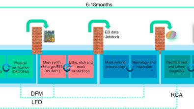
Digital twins facilitate realistic simulations and validations of products, machines, lines, and complete fabs. This sets the stage for flexible and efficient manufacturing, as depicted in figure 1.

The Calibre Fab Insights platform
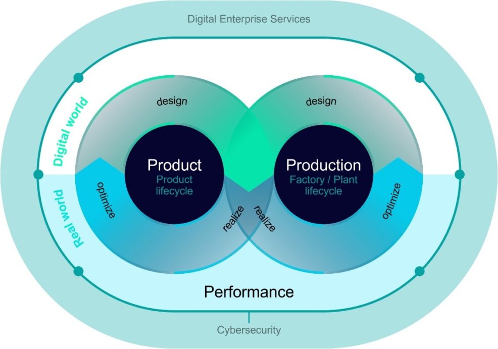
Implementing a digital twin requires a platform that allows simulations and validations of all manufacturing components. Calibre Fab Insights achieves this by exchanging information between different elements, as depicted in figure 2. Calibre Fab Insights provides intelligent solutions utilizing fab-generated data to create ML-based predictive models. It focuses on design-aware feature extraction, virtual metrology with real-time monitoring, and AI-guided recipe setup.
Figure 2. Calibre Fab Insights leverages fab manufacturing history and process sequence to achieve the target yield, providing actionable and predictable data to improve cost and resource efficiency.
Digital twin for the product
As we approach molecular dimensions, understanding the impact of chip topology becomes crucial. While incorporating design characteristics in semiconductor manufacturing is not new, our recent collaboration with GLOBALFOUNDRIES shows the benefits of bringing design content into recipe setup, process monitoring, and yield analysis, and how incorporating design content is a necessary step to successfully implement machine learning technologies in the manufacturing line.
Calibre Fab Insights analyzes design features to identify, rank, and focus on the most impactful aspects, improving process control and wafer dispositioning. Fabs can use the information from the Calibre Fab Insights analysis to:
- Process recipe optimization for new product introduction in the fab enabling reduction in monitoring wafers.
- Identify root cause for excursions and yield detractors.
- Monitor and differentiate between product mix and process drift.
Digital twin for metrology
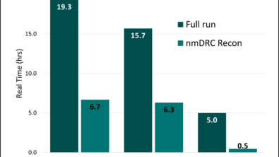
Semiconductor manufacturing involves hundreds of processes, making measuring every wafer’s quality after each process impractical. Metrology, as employed for product quality monitoring tool today, covers only a small fraction of sample wafers. Virtual metrology, on the other hand, lets us predict every wafer’s metrology measurements based on production equipment, data and preceding metrology results. Calibre Fab Insights introduces a new concept called Cross-metrology Assisted Virtual Metrology that uses the experimentally measured points from all designs across all wafers to find the virtually measured point.
In an ideal world, you would understand every field across the wafer to assist in process improvements and per-design process control. However, today metrology data is very sparse. With a digital twin approach using virtual metrology, you can use existing experimental measured points of the design as anchor/correlation points and use adjacent experimental points from all designs across all wafers (figure 3). This virtual metrology system helps monitor and detect early drift of process thereby helping improve product quality, reduce costs, and minimize cycle time.
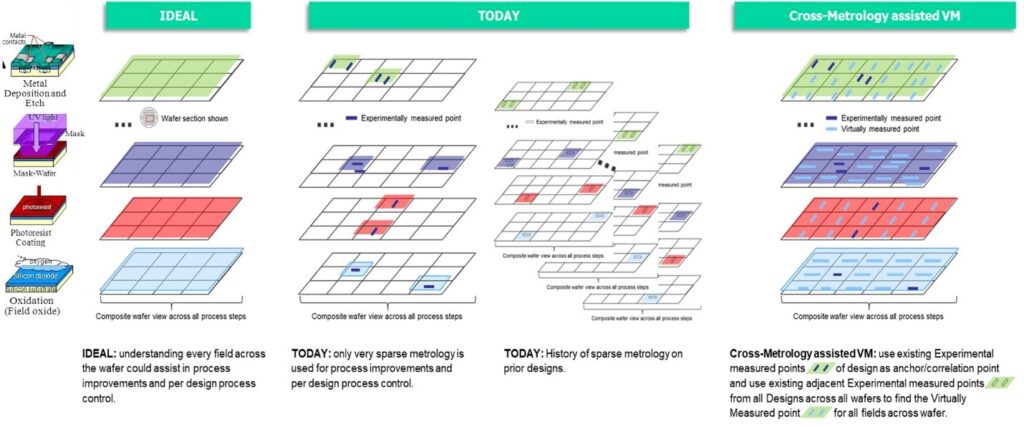
Figure 3. Virtual metrology solves the problem of sparse metrology data available today.
Implementing a digital twin: Digital threads for high-volume manufacturing
Siemens achieves digital twin implementation through digital threads or apps, representing building blocks of the digital twin journey. These threads, including process modeling, tool monitoring, and cross metrology, provide a flexible and scalable solution for high-volume manufacturing. The flexibility of this platform to work in the cloud and/or on-premise along with the scalable nature to be able to deploy across all relevant manufacturing points makes this an adaptive and cost-effective choice.
Conclusion
The digital twin revolution in semiconductor manufacturing, as presented by Siemens’ Calibre Fab Insights, helps provide actionable and predictable insights to improve cost and resource efficiency for high-mix, high-volume manufacturing. By incorporating the fab manufacturing history along with new product info, it leverages process sequence to achieve fab goals including earlier starts, higher initial yields, faster yield ramp, minimized excursions due to improved root cause analysis and, ultimately, higher yield entitlement. As the semiconductor industry embraces this transformation, the benefits of predictive design and process insights become the cornerstone for success in an increasingly competitive landscape.
For more details, read our technical paper Enable smart manufacturing in semiconductor fabs with predictive design and process insights.