How to extend DTCO for today’s competitive IC landscape
By Le Hong
As semiconductor components continue to shrink, the challenges associated with design-for-manufacturing (DFM) and design-technology co-optimization (DTCO) increase. The complexity of the IC design and manufacturing process demands an extension of traditional DFM and DTCO techniques to overcome the systematic failures tied to complex design-process interactions.
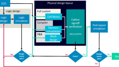
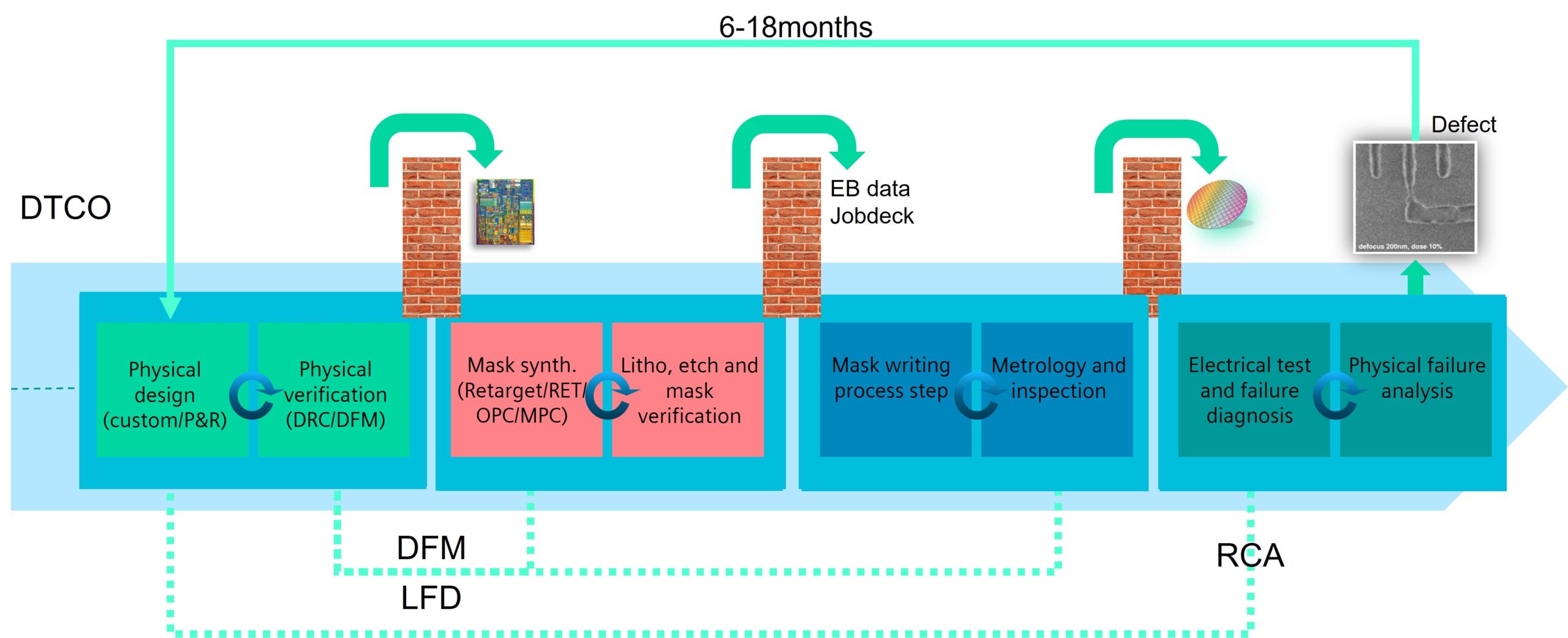
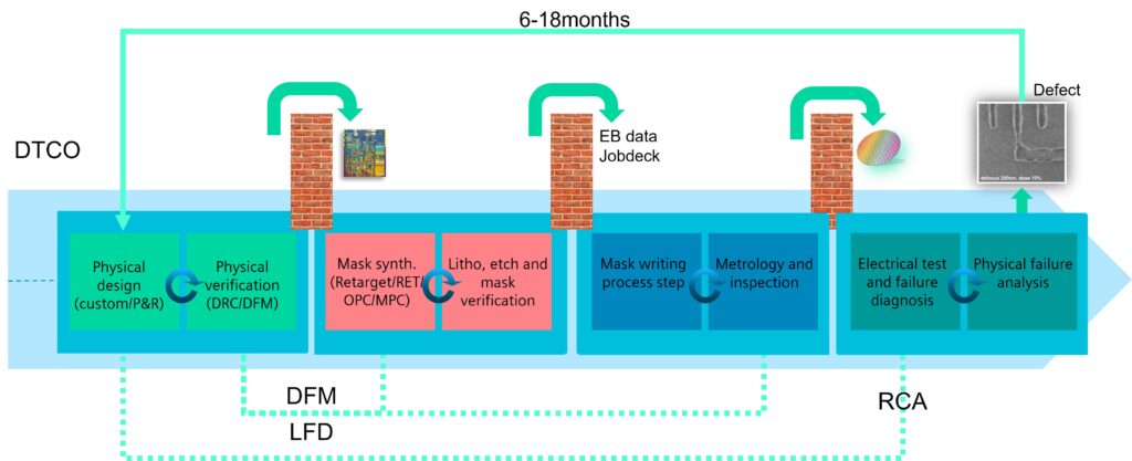
The IC design-to-manufacturing flow has well-defined modules such as physical design, mask synthesis, mask writing, fab process and inspection and test. Each module includes industry-standard verification processes, such as physical verification, optical process correction and mask proximity correction (OPC/MPC) verification, metrology inspection and physical failure analysis (PFA). The communication between these modules is one-directional handoff, as shown in figure 1.
Traditional DTCO
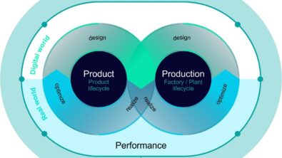
DTCO is critical for yield breakthrough and product ramp-up during the life cycle of a new technology node. It involves the simultaneous optimization of the chip design and manufacturing process, considering the interdependence between the two. It uses iterative design and manufacturing simulations to identify optimal design and manufacturing parameters.
Later in the process node’s lifecycle, such co-optimization is done by traditional techniques like design-for manufacturability (DFM) and litho-friendly design (LFD). But with the shrinking manufacturing technology and growing design complexity comes greater challenges that existing DFM and DTCO can’t overcome.
Limitations of traditional DTCO
Traditional DTCO, DFM and LFD approaches all have proven value, but many designs need more. The truth is that ever more systematic defects escape traditional detection methodology and show up during the yield ramp and final high-volume manufacturing (HVM). To improve the efficiency and effectiveness of the DFM and DTCO processes for complex, advanced node designs, the industry needs more than piecemeal solutions or band-aids.
Extended design-technology co-optimization
Because DTCO is so critical to the definition of a process node, Calibre group at Siemens EDA started researching ways to extend DTCO further, to the entire design-to-manufacturing process by creating a robust information channel. This infrastructure helps get the massive amounts of data where it needs to go to be useful. Our improved and extended DTCO solutions is based on a systematic information exchange and analytics platform that spans various design-to-manufacturing modules with complete lifecycle support. It offers methodologies and infrastructure needed to feed pre-silicon design data and intelligence forward into the manufacturing process, and feed manufacturing information back, post-silicon, to inform the design process. These technologies are available in the Fab Solutions product family.
Figure 2 illustrates the extended DTCO flow we developed. This flow uses ML to give easier access to patterns, locations, properties, distribution, etc. across modules.
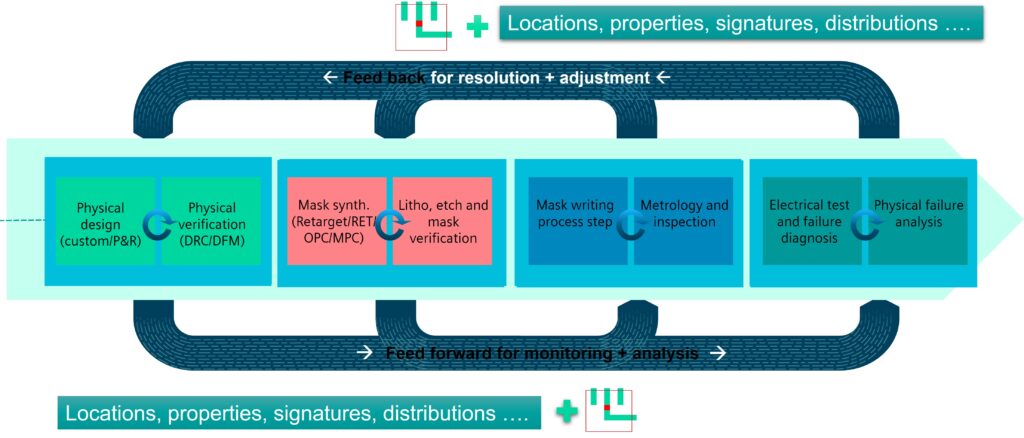
The Fab Solutions products address related issues, such as managing the massive amounts of data generated through the flow and how to bring design content in to process optimization.
CONCLUSION
The semiconductor industry will benefit from extending DTCO from technology development to HVM. Implementing far-reaching design and process co-optimization has already shown promising results in several applications, suggesting that it may lead to a new era of extended DTCO. Calibre Fab Solutions products are leading the way in the use of ML technology to create the Fab Solutions products. The improvements in design and process co-optimization using ML is exciting, as it could lead to remarkable improvements in the quality, speed, and efficiency of semiconductor manufacturing.
To learn more about Calibre Fab Solutions, read the whitepaper Extending design technology co-optimization from technology launch to HVM
You can also watch this presentation about Calibre Fab Solutions or visit our website with more information