Part 3: The 2014 Wilson Research Group Functional Verification Study
FPGA Effort Verification Trends (Continued)
This blog is a continuation of a series of blogs related to the 2014 Wilson Research Group Functional Verification Study (click here). In my previous blog (click here), I focused on the controversial topic of effort spent in FPGA verification. This blog continues that discussion. I stated in my previous blog that I don’t believe there is a simple answer to the question, “how much effort was spent on verification in your last FPGA project?” I believe that it is necessary to look at multiple data points to truly get a sense of the real effort involved in verification today. So, let’s look at a few additional findings from the study.
Time FPGA designers spend in verification
For projects that have a separation of teams (i.e., design engineers and verification engineers), it’s important to note that FPGA verification engineers are not the only project members involved in functional verification. FPGA design engineers spend a significant amount of their time in verification too, as shown in Figure 1.
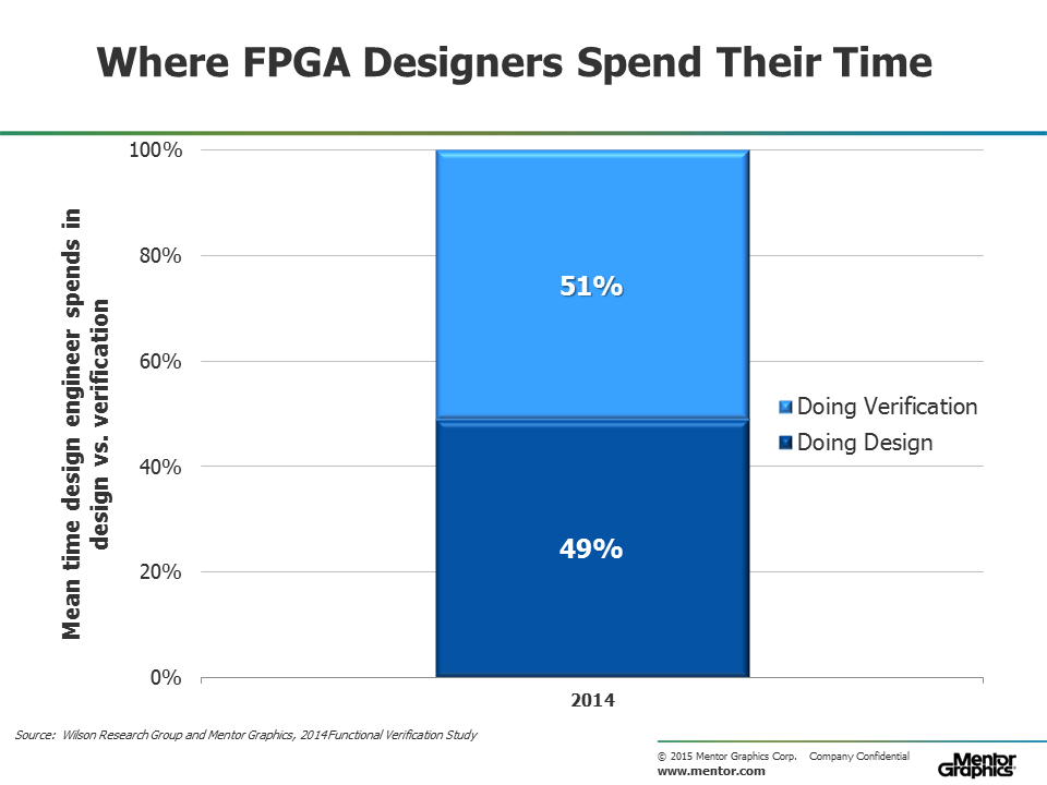
Figure 1. Average (mean) time FPGA design engineers spend in design vs. verification.
You might note (on average) that FPGA design engineers actually spend slightly more time doing verification than design. We are not showing trends here since we have insufficient data related to the questions for FPGA designs from our previous study. We anticipate being able to show trends after our next study (currently scheduled for 2016).
Even if the FPGA project has a separation of teams, the designers are still involved in the verification process, ranging from:
- Small sandbox testing to explore various aspects of the implementation
- Full functional testing of IP blocks and SoC integration
- Debugging verification problems identified by a separate verification team
In fact, getting a better understanding of exactly where FPGA designers spend their time has led us to conduct a series of follow-on discussions with various FPGA projects from various market segments. Through this process we have learned a concern by many project managers related to the increase amount of debugging time spent on a project (both pre-lab and lab debugging time). This is one area of FPGA verification that we plan to continue to explore through a series of in-depth discussions with multiple FPGA projects around the world.
Percentage of time FPGA verification engineers spends in various task
Next, let’s look at the mean time FPGA verification engineers spend in performing various tasks related to their specific project. You might note that verification engineers spend most of their time in debugging. Ideally, if all the tasks were optimized, then you would expect this. Yet, unfortunately, the time spent in debugging can vary significantly from project-to-project, which presents scheduling challenges for managers during a project’s verification planning process.
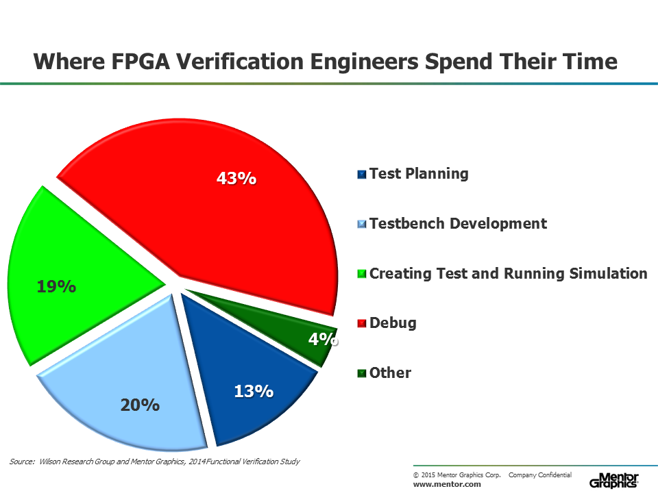
Figure 2. Average (mean) time verification engineers spend in various task
In our 2012 study we found that FPGA verification engineers spent about 37% of their time involved in debugging task. There was a 16 percent increase in the amount of time spent in debugging between 2012 and 2014. Hence, the data suggest that debugging effort is increasing for both FPGA engineers.
In my next blog (click here) I present our study findings in terms of FPGA schedules, iterations in the lab, and classification of functional bugs.
Quick links to the 2014 Wilson Research Group Study results
- Prologue: The 2014 Wilson Research Group Functional Verification Study
- Understanding and Minimizing Study Bias
- Part 1 – FPGA Design Trends
- Part 2 – FPGA Verification Effort Trends
- Part 3 – FPGA Verification Effort Trends (Continued)
- Part 4 – FPGA Verification Effectiveness Trends
- Part 5 – FPGA Verification Technology Adoption Trends
- Part 6 – FPGA Verification Language and Library Adoption Trends
- Part 7 – ASIC/IC Design Trends
- Part 8 – ASIC/IC Resource Trends
- Part 9 – ASIC/IC Verification Technology Adoption Trends
- Part 10 – ASIC/IC Language and Library Adoption Trends
- Part 11 – ASIC/IC Power Management Trends
- Part 12 – ASIC/IC Verification Results Trends
- Conclusion: The 2014 Wilson Research Group Functional Verification Study


Comments
Leave a Reply
You must be logged in to post a comment.
Hi,
Concerning debugging, can you provide finer granularity into the type of debugging that is being done? Does “debugging” just include debugging in the lab, or does that also include RTL debugging?
Thanks,
Roger
The debugging time is this study represents pre-lab (e.g., simulation, formal, etc.). It also represent debugging both the testbench and the design.