Screen shot of the Innovator3D IC canvas

The smart path to STCO with Hierarchical Device Planning (HDP)

Siemens partnered with Intel Foundry to develop a STCO centric capability that enables a “smart path” to homogeneous disaggregation using Hierarchical Device Planning and parameterized pin regions.

chiplet integration with STCO system technology co optimization

Resolving Design Fragmentation Challenges in Chiplet Integration with STCO

Are you struggling to integrate chiplets into an advanced packaging platform due to design fragmentation challenges? The complexity of managing…

The evolution of machine learning (ML) in the physical design and verification of semiconductor packages

Discover how Siemens’ EDA evolution of machine learning in the physical design and verification of semiconductor packages.

Impacts of 3D IC on the future

3D IC technology development started many years ago well before the slowing down of Moore’s law benefits became a topic…

system technology co-optimization

Shifting left with system technology co-optimization for IC packaging

We have witnessed and learned about the industry’s significant shift in semiconductors. The traditional approach of transistor scaling, once universally…

Illustration of 3D IC design workflows

Why co-design-driven semiconductor package planning and prototyping is critical for design success

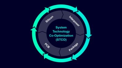
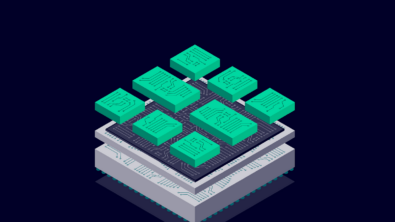
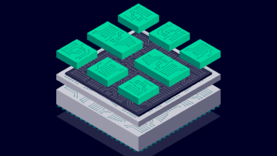
The connectivity management complexity of package assemblies where multiple chiplets/ASICs and memory are heterogeneously integrated, introduces a great deal of…