User2User 2024: EMIB based advanced packaging flow – Intel Foundry

In this User2User 2024 session entitled, EMIB based advanced packaging flow – Zain Ali, IC Packaging Application Engineer at Intel Foundry discusses an advanced packaging flow for multi-die heterogeneous integration using EMIB (Embedded Multi-die Interconnect Bridge) technology.
Zain also explains the transition from traditional silicon interposers to EMIBs, highlighting their advantages in package design complexity and scalability. The presentation covers the technical challenges, design methodologies, and the integration of EMIBs in system-level package designs using Siemens solutions for planning, verification, and implementation.
What is EMIB?
Embedded Multi-die Interconnect Bridge (EMIB) is a semiconductor packaging technology that uses a small, embedded silicon bridge to interconnect multiple dies or chiplets within a single package. Unlike a large silicon interposer, the EMIB bridge only spans the area needed to connect the specific dies, making it a more compact and cost-effective solution. EMIB allows for the integration of multiple dies in a highly integrated system-in-package, with the ability to have multiple EMIB bridges within a single package. This approach requires close co-design of the dies, EMIB, and overall package architecture to optimize performance and cost, in contrast to the more interface-oriented silicon interposer.
What are the challenges with EMIB package design?
The increased design complexity with EMIB technology shifts more of the challenges to the package level. Key issues include supporting high pin counts, integrating diverse components, and accurately representing the EMIB structure in package design tools. Defining the EMIB component modules and setting up constraints to achieve low latency design rule checks (DRCs) is crucial, as EMIB is a passive bridge without active silicon. Power delivery to the EMIB bridge is a primary design concern, requiring point-to-point connections and ensuring sufficient power distribution.
The lack of mature IC package co-design tools, flows, and methodologies has been a challenge in the early adoption of EMIB technology
Zain Ali, IC Packaging Application Engineer at Intel Foundry
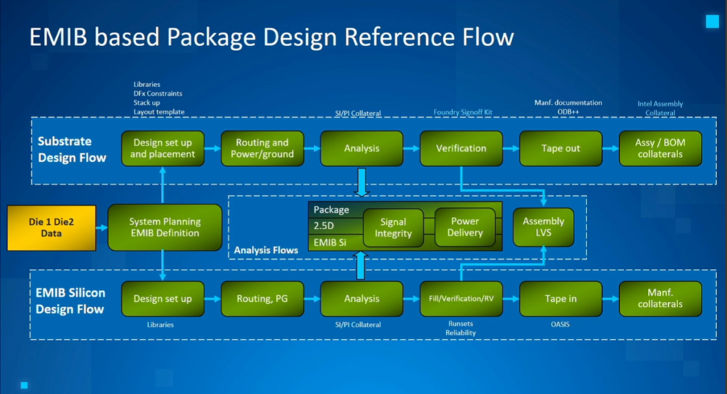
What does an EMIB reference flow look like?
The EMIB-based package design reference flow involves integrating die data, using a system planning tool like Siemens xSI for bump management, and co-designing the package substrate and EMIB silicon simultaneously. The EMIB silicon is routed using a custom tool, focusing primarily on power delivery optimization and analysis, rather than complex routing. The package design follows standard high bump count flows, with the EMIB integrated and analyzed as part of the complete system. Key challenges include managing EMIB constraints, power delivery, and ensuring the EMIB and package designs align through comprehensive co-analysis using tools like 3DSTACK. This integrated, co-design approach is crucial for successful EMIB-based package implementation
What is available for EMIB from Intel Foundry?
As part of the Intel Foundry offering for EMIB technology, a comprehensive set of collaterals is provided to enable successful EMIB-based package design. This includes a silicon PDK (Process Design Kit) with standard libraries, models, and verification flows, as well as an EMIB-specific assembly LVS (Layout Versus Schematic) flow. Additionally, design guides and a reference EMIB design are made available. On the package side, a PADK (Package Assembly Design Kit) includes BGA templates, a foundry sign-off kit, a reference package design, and an EMIB integration guide for the package layout. The key emphasis is on the need for tight co-design between the EMIB silicon and the package, as the power delivery network is critical and must be carefully coordinated across the integrated system.
EMIB Design implementation with Siemens
Designing an EMIB-based package involves coordinating the requirements between the silicon and package domains. On the silicon side, the EMIB bump pattern must meet the design and assembly needs, along with providing the necessary die-to-die connectivity netlist. The package side requires designing the bump pattern to compensate for scaling and manufacturing constraints, especially when multiple EMIBs are integrated within a single package. This includes defining the EMIB placement, such as in a cavity, and the EMIB package connectivity netlist. The system planning tool, like xSI, plays a crucial role in managing these separate but interdependent netlists for the silicon and package, enabling the co-design and co-optimization of the EMIB and the overall package. Finally, the design process culminates in the assembly and test of the complete EMIB-based package.
What’s next?
Watch the video recording now available on demand to learn more about Siemens’ EMIB-based package design flow leveraging the Xpedition IC packaging suite, including xSI for system planning and Calibre 3DSTACK for 3D co-analysis. You’ll also discover how a package-centric approach enables the co-design of EMIB dies, routing, and system-level verification to address the increasing complexity of advanced packaging.
If you missed User2User 2024 or attended the event and want to watch the 3D IC sessions again, the library of videos is now available on-demand here: Click here
To learn more about Siemens EDA 3D IC solutions, visit our 3D IC Homepage