Automated analysis-based layout enhancements reduce power grid voltage drops during place & route: A case study with Google
By Jeff Wilson
Power isn’t just a small factor in the IC design arena—it’s a cornerstone. Design teams work to hit the trifecta of power, performance, and area (PPA) targets that reflect the intended market and functionalities of their products. The journey from concept to physical implementation is one of precision and innovation, as these teams shape layouts that meet these stringent targets. But, as technology pushes into more advanced process nodes, striking a balance between effective power management and optimal performance and area is becoming an increasingly complex challenge.
At the heart of IC functionality is the need for power to operate correctly. This means ensuring that the electricity flowing through an IC’s wires always meets minimum voltage requirements. However, when this current encounters resistance, it leads to what’s known as an IR drop—a reduction in voltage that can jeopardize the entire circuit’s functionality.
Take Google’s experience as a case in point. During their work on a cutting-edge 5 nm design, they ran into vexing voltage (IR) drop issues. The team’s initial attempts to tackle these problems with traditional place and route (P&R) strategies and manual tweaks turned out to be a series of time-consuming iterations that drained significant engineering resources. What they needed was a precise and efficient approach to layout optimization that could minimize IR drop violations without sidelining their performance or area goals.
Enter Siemens EDA’s Calibre DesignEnhancer. This tool emerged as a game-changer for Google, offering a push-button solution that revolutionized their design process. With Calibre DesignEnhancer, Google’s team was able to dramatically reduce IR drop issues, streamline their design implementation, and ensure that their final product not only met but exceeded their power management expectations.
The challenge of IR drop in advanced IC designs
One of the key hurdles in IC power management is mitigating voltage reduction across interconnects, known as IR drop. This issue arises primarily due to two factors:
- Static IR Drop: As devices become smaller, the wires within ICs become narrower, increasing their inherent resistance and causing a drop in voltage along the path.
- Dynamic IR Drop: High switching activity among transistors can lead to localized high current zones, which exacerbate voltage drops and can lead to performance degradation or even functional failures.
For example, Google faced significant IR drop challenges during the development of a 5 nm design, struggling with the time-consuming process of manual adjustments and iterative place and route (P&R) solutions.
Innovative solution by Siemens EDA: Calibre DesignEnhancer
To overcome these challenges, Google turned to Siemens EDA’s Calibre DesignEnhancer, an automated tool designed to optimize layout and minimize IR drop issues efficiently and effectively. This tool integrates seamlessly with existing P&R solutions, providing a user-friendly, push-button solution that drastically cuts down the time and resources needed for layout optimization.
Key features of Calibre DesignEnhancer
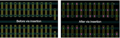
- Via optimization and power grid enhancement: The tool includes functionalities like via optimization and power grid enhancement. It automatically adds DRC-clean vias and creates parallel run lengths in the layout to reduce resistance and enhance power integrity.
- Ease of use and integration: Calibre DesignEnhancer is compatible with all major IC design tools, minimizing training and support requirements while allowing designers to work within their preferred environments.
- Read a thorough introduction to Calibre DesignEnhancer here.
Case Study: Google’s implementation and results
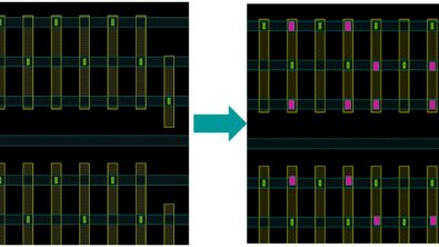
Google utilized two primary functionalities of the Calibre DesignEnhancer—via insertion and power grid enhancement—to address its IR drop challenges in a 5 nm IC design:
- Via insertion: Automated via insertion helped to reduce the via resistance significantly, thus enhancing manufacturing robustness and reliability.
2. Power grid enhancement: By creating parallel run lengths of DRC-clean metal and vias, the tool effectively lowered resistance in the power grid structures, directly addressing the identified IR drop hotspots.
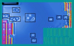
The results were clear: these automated solutions not only reduced the number of IR drop violations significantly but also provided a substantial runtime advantage over traditional P&R methods.
Conclusion: The future of IC design with automated EDA tools
The integration of automated tools like Calibre DesignEnhancer into IC design workflows represents a significant advancement in electronic design automation. These tools not only simplify complex processes but also ensure that designs meet stringent power, performance, and area requirements with greater efficiency and less manual intervention. As the industry continues to evolve, the adoption of such automated solutions will be key to meeting the ever-increasing demands of IC design and manufacturing, ensuring that design teams can achieve their PPA targets reliably and efficiently.
Traditional approaches to tackling inherent challenges like IR drop have often been laborious and less than fully effective. Confronted with these hurdles, Google was on the lookout for a more efficient, precise solution to tackle IR drop challenges in their 5 nm design. Their teamwork with Siemens EDA brought forth the Calibre DesignEnhancer Via and Pge design flows, offering a suite of automated solutions that effectively minimized IR drop violations during the physical implementation stage.
If you want to read more about this collaboration, we also have a technical paper available, Google reduces IR drop issues with analysis-based layout enhancements (siemens.com)