Unraveling the 3DIC shift left strategy: Navigating the world of multi-dimensional ICs
By John Ferguson
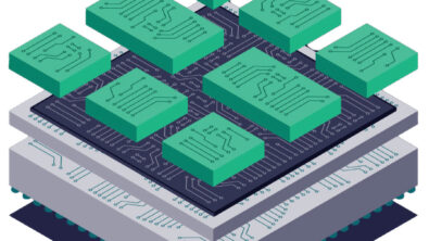
IC design’s evolution continues to push the boundaries of Moore’s law to new heights. One of the most intriguing developments in recent years has been the rise of multi-dimensional 2.5D and 3DICs. Unlike traditional ICs, these designs are composed of multiple individual chiplets, each optimized for a specific purpose. The challenge for designers lies in connecting these chiplets effectively. Luckily, this becomes a less daunting task by incorporating elements of a shift left strategy within the framework of the 3DIC design flow.
3DIC design options and assembly flow
Designing a 3DIC assembly is a complex journey that starts with the chiplet components. Multi-dimensional ICs offer a myriad of design options for connecting chiplets. Some of the most common approaches include chiplets connected via interposer with bump connections and through-silicon-vias (TSVs), chiplets placed directly on packages, or chiplets stacked on top of each other through various bonding techniques. The flexibility to combine these approaches on a single 3DIC assembly opens up new possibilities, but also introduces unique challenges for designers.
Choosing the right 3DIC floorplan is a crucial first step, as it impacts thermal and mechanical stresses, which in turn affect electrical behavior. This decision-making process often requires multiple iterations to arrive at the optimal design.
Challenges in 3DIC physical verification
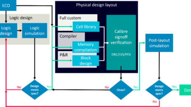
Physical verification (PV) of 2.5/3DIC designs brings novel challenges to the forefront. It begins with verifying each chiplet against its foundry process node requirements, a task similar to verifying individual blocks in a system-on-chip (SoC) design. However, the real deviation from traditional PV occurs during the assembly verification.
For layout vs. schematic (LVS) verification, designers traditionally use a manually created assembly netlist in CSV or spreadsheet format, and decks requiring ‘pseudo-devices, which are prone to human error. Additionally, using separate rule decks for design rule checking (DRC) and LVS for different interfaces within the package can be cumbersome and error prone.
Furthermore, relying solely on interface rule decks makes it practically impossible to generate a full assembly post-layout netlist necessary to understand electrical interactions across multiple components, a critical aspect of verification.
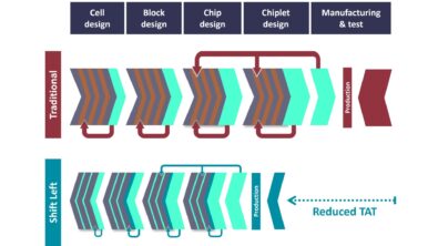
Introducing shift left verification to 3DIC design
To expedite time to market and achieve early volume production of IC designs, Calibre Design Solutions provides innovative tools and functionalities that enable design companies to implement earlier design-stage verification with Calibre signoff accuracy, enhancing productivity and design quality while reducing time to market. It’s as simple and as effective as this graphic shows:
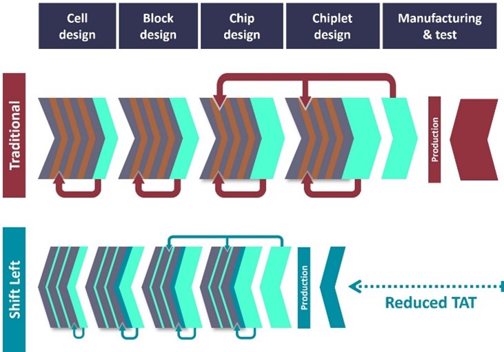
Applying shift left strategies to 3DIC design
Introducing the Calibre shift left strategy to 3DIC design opens new avenues for improving designer productivity, 3DIC design quality, and time-to-market. By embracing this approach, designers can navigate the complexities of multi-dimensional ICs with confidence. Here’s a closer look at how to apply shift left techniques to the 3DIC design flow:
- Utilize Siemens Xpedition™ Substrate Integrator (XSI) software: With XSI software, designers can create 3D floorplans, providing an early opportunity to analyze and rule out configurations that may contain serious flaws. This step helps streamline the design process by eliminating undesirable design options at an early stage. Read more about how the Siemens Xpedition™ Substrate Integrator (XSI) Software has been useful in our video – Simplified physical verification of 3DICs through 3Dblox
- Leverage the Calibre 3DSTACK tool for comprehensive assembly-level post-layout netlists: For successful LVS-level verification, designers must generate a full assembly-level netlist. Designers can extend the already widely adopted infrastructure in place with the Calibre 3DSTACK tool to generate an assembly description that defines the 3D stackup using the Calibre 3DSTACK+ tcl text-based format. For complex assemblies, this description generation can be automated using such tools as the XSI design planning tool. Alternatively, newer formats such as the 3Dblox™ standard can also encapsulate such information. The ability to create this netlist is crucial for ensuring accurate and efficient verification of the entire 3DIC assembly. In addition, the use of the Calibre 3DSTACK tool helps simplify the 3DIC verification process, making it more efficient and less prone to errors. This automation contributes to the overall success of the 3DIC design.
- Streamline verification with single runs: With a complete assembly description, the Calibre engine can understand the connectivity and geometric interfaces across all components in the assembly, enabling a single deck and single run to not only identify and display DRC and LVS issues in a single results output, but also use the data captured during the individual chiplet-level LVS and similar runs, combined with the top assembly-level extraction data, to generate a post-assembly netlist for further analysis. Consolidating these tasks into a single step enhances efficiency and ensures comprehensive verification of the 3DIC assembly. This understanding of the assembly can also drive automation of cross-die parasitic coupling impacts and enable full assembly analyses, including not only ESD and antenna issues, but also extending to capture thermal and mechanical stress impacts on the 3DIC electrical behavior.
Addressing thermal and mechanical stresses
Mechanical stresses and temperature changes significantly impact electrical behavior. In traditional IC/SoC designs, safeguards are in place, but 3DIC assemblies introduce new challenges. Innovative capabilities in the Calibre tool suite capture electrical impacts of both thermal and mechanical stresses. The Siemens mPower™ solution aids in creating the initial power network, facilitating thermal analysis using Calibre 3DThermal technology. This technology generates accurate thermal maps that can be used to drive thermal analysis. Adding corresponding mechanical stress properties for each of the materials across the full assembly to the assembly stack-up definition enables 3DIC designers to generate a stress map. Boththermal and stress impacts can be passed to device-level netlists for accurate post-assembly simulations.
Iterative cross-simulation
Thermal and mechanical stresses are interconnected, creating a complex web of interactions. Designers address these challenges through iteration, using power maps to drive thermal and stress map extraction, and, more importantly, generation of post-layout netlist which is inclusive of the electrical impacts. This can then be fed downstream for spice-level simulation, static timing analysis, or EMIR analysis.
Early assembly verification
Identifying and addressing issues earlier in the design flow is essential for more successful 3DIC design. As design components mature and more detailed models become available, iterations become more accurate. Earlier assembly verification helps designers make informed choices and achieve confidence in their 3D heterogeneous assembly designs.
Conclusion
In the world of 3DIC design, a comprehensive understanding of the entire system is vital. The shift left strategy supported by Calibre Design Solutions and Siemens EDA tools streamlines the 3DIC verification process, providing designers with a holistic approach. Early assembly verification empowers designers to make informed decisions and ensures the success of 3DIC designs. Embracing these innovative approaches, designers can navigate the complex world of multi-dimensional ICs with confidence.
For more details, read our technical paper: Reduce 3DIC design complexity with early package assembly verification