3DICs and the multi-physics challenge
By John Ferguson
Design teams have known since, well, pretty much forever that mechanical stresses and temperature changes can affect electrical behavior. These impacts change device mobilities and conductivities in active devices, as well as impacting resistivities and electromigration impacts in passive devices,. In traditional integrated circuit (IC) or system-on-chip (SoC) designs, these impacts are largely safeguarded by the fact that all devices are on a common silicon die. With a few appropriate design rules to keep devices sufficiently separated from local impacts, designers can ensure that most impacts are minimized or avoided. Simply by extracting some additional device parameters, further gross deficiencies can be flagged for review, enabling any additional concerns to be captured during post-layout simulation. Unfortunately, when it comes to the world of 3DIC design, those safe-guards are no longer practical.
Traditional IC and SoC designs vs. 3DIC challenges
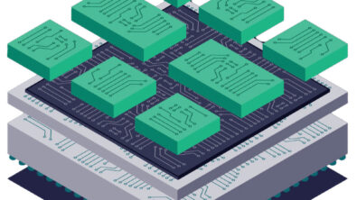
Unlike the IC world, 2.5D and 3DICs are composed of multiple individual chiplets, each of which may be built to a separate process node best suited for their specific purpose.
Diverse connection methods in 3DICs
There are multiple ways in which these chiplets can be connected:
- chiplets connected via interposer with bump connections and through-silicon-vias (TSVs)
- chiplets on package
- chiplets on packages with discreet and thinned interposers embedded without TSVs
- chiplets stacked on chiplets through direct bonding techniques
- chiplets stacked on chiplets with TSVs or copper pillars and more bumps
Furthermore, any or all of these approaches can be combined on a single 3DIC assembly. This plethora of options results in multiple components of different materials integrated in all three dimensions, introducing new stresses and impacting access to thermal heat sinks. There are also new thermal impacts coming from the manufacturing processes as well as from providing power and active device toggling. All of these effects together create several new verification challenges for 3DIC designs.
Addressing verification challenges in 3DIC designs
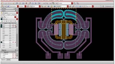
The most obvious challenge is how to ensure that the active chiplets in a 3DIC assembly will behave electrically as intended. Calibre Design Solutions addresses this issue by extending the already widely adopted infrastructure in place with the Calibre® 3DSTACK tool to define the 3D stack-up. This definition can be created using rule deck syntax, automated with the Siemens Xpedition™ Substrate Integrator (XSI) platform, or automatically translated from the 3Dblox™open format. Having this insight allows the Calibre engine to understand the connectivity and geometric interfaces across all components in the assembly, ultimately enabling a single deck and single run to identify design rule checking (DRC) or layout vs. schematic (LVS) issues, and to generate a post-assembly netlist for further analysis. This definition can also drive automation of cross-die parasitic coupling impacts, which lays the groundwork for 3D-level analysis of thermal and stress impacts.
Defining the 3D stack-up for 3DIC assemblies
The first step is to create the initial power network. The Siemens mPower™ solution can use the generated output of the 3DSTACK run to extract the connectivity and any coupling across the chiplets. Adding the individual chiplet networks and internal connectivity to this data allows for the creation of power maps that can be used to drive thermal analysis.
Power network and thermal analysis in 3DICs
3DIC thermal analysis can be performed using innovative Calibre technology. Using the same assembly definition created for the 3DSTACK connectivity extraction, together with appropriate materials property definitions for each component as well as any boundary conditions, this functionality leverages the widely adopted Simcenter™ Flotherm™ thermal solver to generate the thermal maps needed. Because the Calibre software has all the detailed layer information for the individual chiplets, it can generate very accurate individual die thermal models. Additionally, by leveraging the chiplet-specific layout and connectivity, those thermal impacts can be transformed to the device-level, enabling accurate post-assembly simulations or electromigration and voltage (EMIR) analysis.
Capturing electrical impacts of mechanical stresses
Similarly, new Calibre capabilities enable the capture of electrical impacts of all stresses on the active chiplets. Using the same assembly stack-up definition used for the initial Calibre 3DSTACK runs and the corresponding mechanical stress properties for each of the materials across the full assembly, a stress map is generated. As in the case of the thermal analysis, these stresses can be pushed down to the device level to enable accurate post-assembly simulation and analysis at the active chiplet levels.
Interplay between mechanical stress, thermal impacts, and electrical behavior
However, these impacts cannot be treated in isolation. Mechanical stresses induce heat. Thermal impacts induce mechanical stress. Both thermal and mechanical stresses impact electrical behavior, which can, in turn, generate more heat. Mitigating these impacts can be largely addressed through iteration. A power map can be used to drive extraction of a thermal map, which can be passed to augment the stress maps. Stress and thermal impacts can be passed to device-level netlists for simulation, updated EMIR analysis, etc. Ultimately, this level of cross-simulation can be automated for 3DIC design teams. However, even that amalgamation of thermal and mechanical stress verification is insufficient. If final signoff verification finds issues, it is essentially too late to make sufficient modifications to the assembly to address them!
Early design analysis and 3DIC floorplan selection
How can these issues be identified and addressed earlier in the design flow? Further, how can designers select the 3D-floorplan that best supports optimal electrical behavior?
Fortunately, there is an answer for both of these questions!. Using a tool like XSI, designers can specify several different 3D floorplan options. While not all the detail for all layers and materials will be available, this approach enables sufficient early analysis to help rule out configurations with serious flaws. Using uniform materials, and simplified or uniform power maps, designers can at least eliminate undesirable design configurations from consideration. As design components begin to mature with chiplet or interposer level DEF data and generic published materials properties, further iterations can become more accurate. As individual chiplets or interposers achieve their full layout, more detailed models can be generated. Pre-existing chiplets, or even sub-assemblies, can have their thermal maps captured in standard formats like ECXML, ultimately simplifying and speeding the analysis required when the chiplets are placed in context of the assembly. In this way, by the time final iteration is performed, designers should encounter very few (if any) late-stage issues.
Proven solutions for ensuring successful 3DIC designs
While 3DIC design clearly brings a great deal of promise to the design world in terms of size, performance, power, and costs, it also introduces some significant new verification challenges. As the industry comes together to address these challenges, we can expect to see even more improvements in this domain. In the meantime, 3DIC designers can rest assured that there are proven solutions in place to help ensure 3DIC designs not only meet manufacturability requirements, but also properly implement the intended electrical behavior.
For more information about 3DIC verification, check out some of our 3DIC technical papers:
Successful 3DIC design, verification, and analysis requires an integrated approach
Taking 2.5D/3DIC physical verification to the next level
Reliability verification in 3D IC designs
2.5D/3D IC latch-up prevention: an automated verification strategy
System-level connectivity management and verification of 3D IC heterogeneous assemblies