Efficient Parasitic Extraction Techniques for Full-Chip Verification
By Yousry Elmaghraby, Mentor Graphics
Choosing the best PEX method for your full-chip or SoC design is essential. But how do you know which one is best?

Ever since the idea of building electronic systems using integrated circuits (ICs) was born in 1949, technology has evolved swiftly. Moving from small to very-large-scale integration, transistor count on a single chip has grown from tens to billions of transistors. As technology evolves, feature size gets smaller and the number of stack layers increases, making physical and electrical verification not only more complex, but also more critical throughout the design cycle.
Parasitic extraction and circuit simulation are major challenges in today’s chip-level verification process. While most parasitic extraction tools supplied by electronic design automation (EDA) vendors offer an extraction solution for full system-on-chip (SoC) and full-chip memory designs, the huge device count in these designs, as well as their increasing routing and device complexity, make it tough for SPICE simulators to swallow such a huge network of devices and extracted components at the chip level. Extraction becomes even more challenging for chips that include large LEF/DEF and metal fill macros.
To keep up with this growth in complexity and size, some parasitic extraction engines provide multiple extraction approaches that target different design types, design stages, and circuit verification intentions. Deciding which method to use is a matter of understanding your extraction requirements in the context of the design. Let’s take a look at the options, and why you might choose one technique over another.
The most accurate, yet relatively time-consuming, extraction mode is the “flat” transistor-level mode. In flat mode, extraction details are captured down to the transistor level, and all design cells are flattened to enable the extraction of all interactions between components. However, if you are creating a mixed-signal design with some pre-characterized digital modules, or you have incomplete analog blocks in your design, using the flat mode will not fit your extraction needs because it would result in double-counting these cells, leading to inaccurate results.
Another consideration is the size of the extracted netlist. Real designs often include modules that are repeated multiple times in the layout. For example, extracting a netlist of several gigabytes of memory would significantly increase simulation time, without providing any increase in useful parasitics information. The hierarchical extraction mode provides a way to extract any repeated modules once in isolation, but still capture their total loading effects on routing at higher levels of hierarchy. Extracting such blocks once saves both extraction and simulation run time.
To further minimize netlist size, hierarchical extraction also provides an efficient way to zoom into parasitic details for the most sensitive analog blocks, while giving less focus to parasitic extraction in other static modules in your design. You can define specific modules/nets in the design that can be excluded during extraction, while all other blocks/nets are fully extracted.
Although full-chip verification is still essential for final signoff quality, designers can incrementally extract and simulate the connectivity of different blocks at the chip level during the design and verification flow. This approach provides a fast, yet indicative, view of the loading and coupling effects coming from top-level integration and acting on small blocks. Quick access to this knowledge reduces the turnaround time for multiple verification iterations, helping designers achieve a faster time to market.
Let’s walk through some typical situations where different extraction features and techniques can help quickly capture problems in early stages of your design.
Net-Based Extraction Flow
Net-based extraction can be useful when designers have huge supply and ground nets in their top-level design. Using a “select net” extraction functionality, you can exclude such nets from the extraction process, while still considering their loading effect on surrounding critical nets in your design.
As shown in Figure 1, you can include all cells (red) and all nets (orange) in extraction, while excluding the huge power and ground network (black). In this case, coupling capacitance between power/ground nets and surrounding interconnects is annotated as a capacitance to ground from the surrounding nets in the extracted netlist.
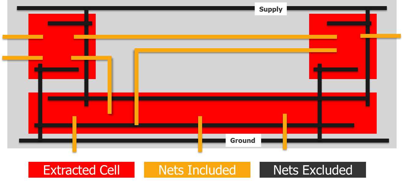
Figure 1. Excluding power nets during extraction helps reduce netlist size.
In the same way, you can select specific net(s) for extraction, while excluding others. Depending on the extraction tool you use, you may be able to automatically include all coupled net(s) to the selected net(s) for extraction as well.
Hierarchical Extraction with Select Net Flow
In some cases, designs may contain blocks that were verified after parasitic extraction, but designers still need to verify timing for connectivity between those blocks on the top level. This timing verification is important to ensure that loading and coupling added after top-level routing don’t affect the overall circuit performance.
To achieve this timing verification, some designers create new cell views by copying the cells involved, and the routing between them, as in the top-level layout view. Occasionally, designers must also add metal resistors and new ports.
Using hierarchical extraction with the select net capability, these extra steps are no longer needed. Figure 2 shows a layout where two cells (red) and the routing between them (orange) are extracted, while all other blocks (blue), and nets (black), are excluded from parasitic extraction. The extracted netlist is generated just for the concerned blocks/nets, including all design blocks/nets and parasitic elements.
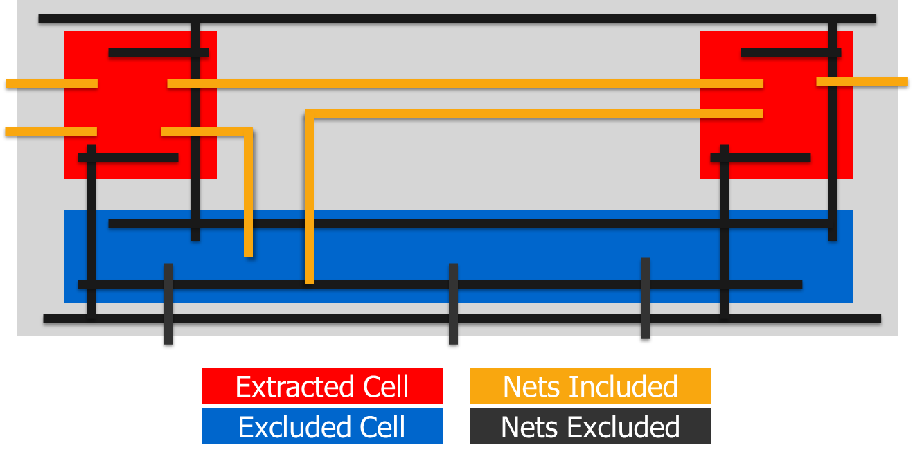
Figure 2. Verify top-level interconnects for specific blocks and nets.
Hierarchical Extraction with In-Context Flow
A hierarchical flow with in-context extraction lets designers extract and generate a netlist for specific blocks in a top-level design, allowing them to simulate a single small cell taking the loading effects of the top level. This cell-extracted netlist includes not only the parasitic elements caused by routing inside this cell, but also any top-level routing effects.
Figure 3 illustrates an example where a single block (red) is included in the extraction, with all interacting nets from the top level (orange) considered. The extracted netlist includes this single cell with its top-level routing effects. The extracted sub-circuit from the in-context extraction flow can then be easily plugged into different netlists or test benches to consider the top-level loading effects for this specific block.
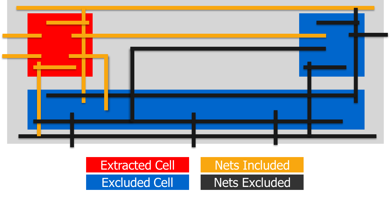
Figure 3. In-context extraction for a single block.
Hierarchical Extraction with Pre-Characterized Cell Definition Flow
When designers use a pre-characterized block from a third party, they don’t want to perform any parasitic extraction on that block, to avoid double counting of extraction effects. In such cases, a hierarchical extraction flow with pre-characterized cell definition can be useful. This flow switches off extraction for those pre-characterized blocks, yet captures coupling capacitance between the cell and the surrounding routing on the higher levels in hierarchy. It also captures coupling capacitance between internal routing in different pre-characterized cells. Using this flow, all integration effects for the pre-characterized cells are captured without extracting those cells.
In Figure 4, three blocks are defined as pre-characterized cells (blue). Coupling between routing inside these cells and the top-level routing (yellow) surrounding these blocks is captured during extraction.

Figure 4 Extracting pre-characterized cells.
As demonstrated, hierarchical and select net extraction flows provide numerous benefits in chip-level verification. Chip-level full parasitic extraction and circuit simulation iterations are expensive in terms of long turnaround verification time. Designers can shorten this loop by choosing from a variety of extraction features that provide an early estimate for how integration will affect the overall chip performance before chip signoff verification.
Author
Yousry ElMaghraby is a Technical Marketing Engineer in the Design to Silicon division of Mentor Graphics, supporting Calibre extraction products.

Liked this article? Then try this –
White Paper: Calibre xACT Parasitic Extraction Supports Signal Integrity at Advanced Nodes
This article was originally published on www.edn.com

Comments
Leave a Reply
You must be logged in to post a comment.
Hi Yousry,
I am curious about the coupling extraction between different PCells. I tried gate extraction on two exact same MOM cap cells close to each other in the same layout. It turns out that no parasitic RC are reported. Is there any other setting I need to switch on ? Thanks!