Parasitic Extraction for Accurate Signal Integrity Analysis at Advanced Nodes
By Karen Chow, Mentor Graphics
Signal integrity analysis at advanced nodes requires new and enhanced parasitic extraction techniques

A number of new models have emerged that are useful for parasitic extraction at advanced nodes, including multi-patterning, FinFETs, and resistance and capacitance models.
When moving to advanced process nodes, such as 16 nm, 14 nm, and 10 nm, creating an accurate model of the chip to enable precise characterization presents many challenges.
Because signal integrity (SI) analysis must address a number of these challenges, including high current, IR drop issues, and crosstalk noise, it is important to have an accurate extracted netlist to use during simulation.
A number of new models have emerged that are useful for parasitic extraction at advanced nodes, including multi-patterning, FinFETs, and resistance and capacitance models.
Signal Integrity
When designers discuss SI on chips, they mean the process of ensuring that the signal passed through the chip maintains its integrity, and is not negatively impacted by any other signals.
For example, coupling capacitance between two long bus lines running parallel to each other can cause a jump in voltage in one line to incorrectly cross over into the other line.
By performing SI analysis, such as measuring crosstalk noise, IR drop, and electromigration, these types of issues can be resolved before a chip is manufactured.
In a typical analog design flow (Figure 1), requirements for each block are defined, circuit design is completed, and the schematic is captured in a design tool.
Next, a simulation is run, using a tool like the Mentor Graphics Analog FastSPICE simulator. After successful simulation, a physical layout is prepared, and both design rule compliance and a layout vs. schematic (LVS) comparison of that layout are run using tools such as the Calibre DRC and Calibre LVS verification software.
To provide data needed for the post-layout simulation, designers then perform parasitic extraction and generate a netlist appending the parasitic resistance and capacitance to designed devices such as transistors. This parasitic netlist is then used for more accurate SI analysis. Any SI issues are returned to the layout team for layout adjustments.
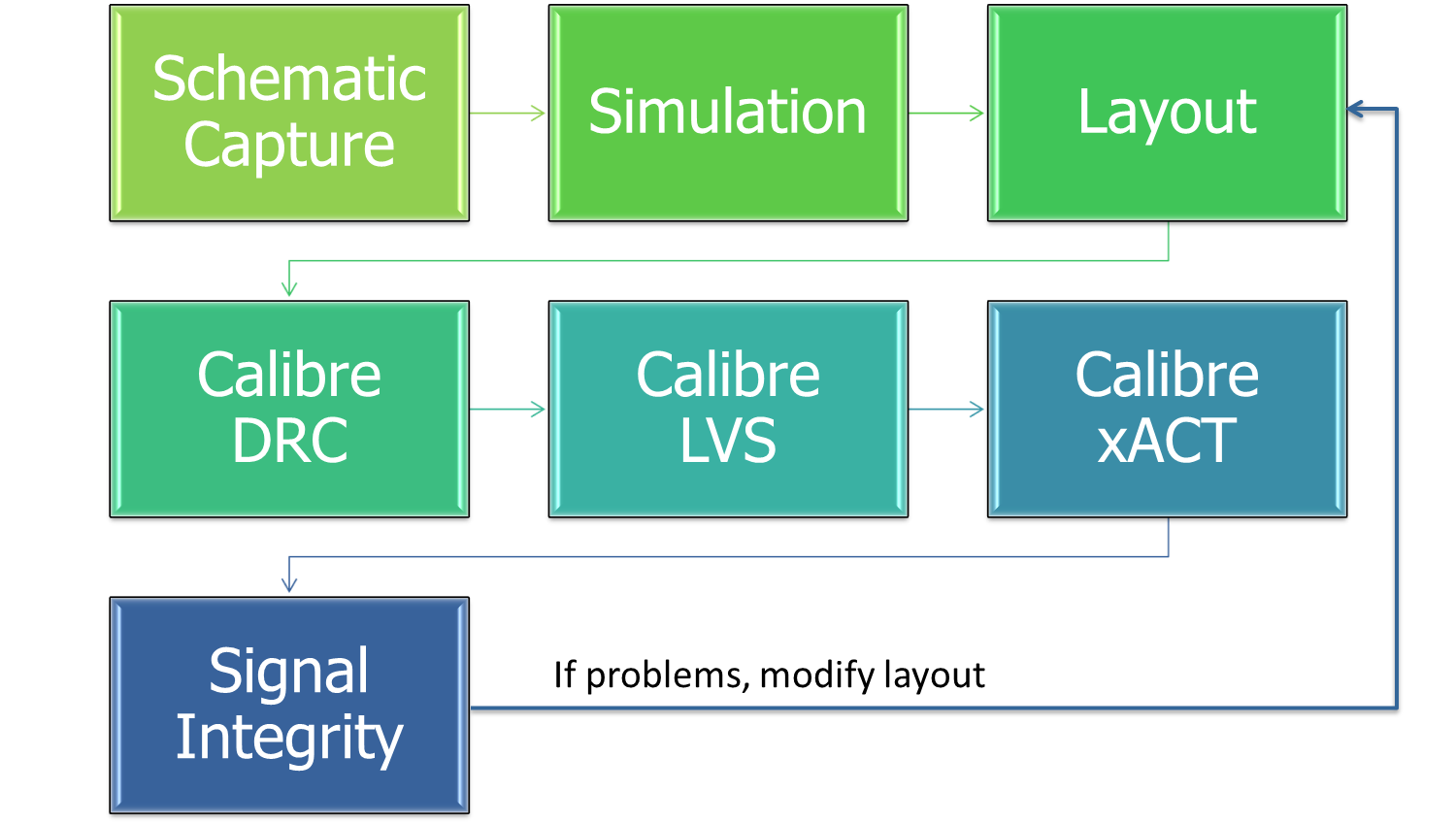
Figure 1. A typical analog design flow, showing schematic capture, layout, verification, parasitic extraction, and post-layout signal integrity analysis.
Parasitic Extraction at Advanced Process Nodes
To perform accurate parasitic extraction at 16 nm, 14 nm, 10 nm, and below, there are many effects that must be considered by the parasitic extraction tool.
To begin with, advanced nodes present new extraction challenges, such as multi-patterned layouts and finFET devices. In addition, the tighter dimensions of these designs create the need for new or expanded extraction techniques.
For example, parasitic coupling capacitors affect crosstalk, so they must be identified. Highly accurate resistance extraction, which can be fed into electromigration analysis, is necessary for measuring current density. Knowing post-OPC interconnect widths is also important for accurate current density calculation.
And lastly, IR drop analysis, which measures how much voltage drop occurs in the power supply due to parasitic resistance and the current flowing through the power (VDD), requires extremely accurate parasitic resistance data.
Multi-patterning
Starting at 20 nm, double patterning is required to print certain layers. At 16 and 14 nm, it is common to have several layers that require double patterning, but to offset increasing mask costs, the foundries often release cost-reduced process types within one node that reduce the number of masks required. This approach is useful for low power designs that don’t require high performance.
At 10 nm, additional multi-patterning techniques must be used. Triple patterning is predicted for some manufacturers, who will use some form of litho-etch- litho-etch-litho-etch (LELELE), while others will employ self-aligned double patterning (SADP).
One of the major parasitic extraction challenges in multi-patterned layouts is mask shift. It is virtually impossible to expose multiple masks in exact alignment, and the resulting variation in spacing can affect electrical characteristics of the design. Identifying and accounting for these mask shifts during parasitic extraction is essential to ensuring accurate electrical characterization of the layout.
At the 16/14 nm nodes, the mask coloring is done by the foundry. This makes it impossible for the extraction process to model the actual mask shifts, since it is not known which polygons belong to which masks.
In this case, the shifts in masks are mimicked as best case/worst case. In the best case example, it is assumed that all conductors will shift farther apart, which is mimicked by making the dielectric constant smaller. In the worst case example, it is assumed that all conductors will shift closer together, which is mimicked by making the dielectric constant larger, in turn making the coupling capacitance value bigger.
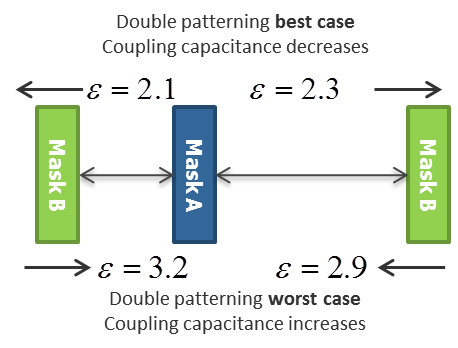
Figure 2. To model this double-patterned layer, the extraction tool changes the space-dependent sidewall dielectric to mimic a capacitance change. Having a lower dielectric constant mimics coupling capacitance decrease, and higher dielectric constant mimics coupling capacitance increase.
For 10nm, some foundries are requiring customers to perform their own mask decomposition. This approach makes it possible for the parasitic extraction tool to more accurately predict whether the coupling capacitance will increase or decrease, by measuring actual mask shifts (Figure 3).
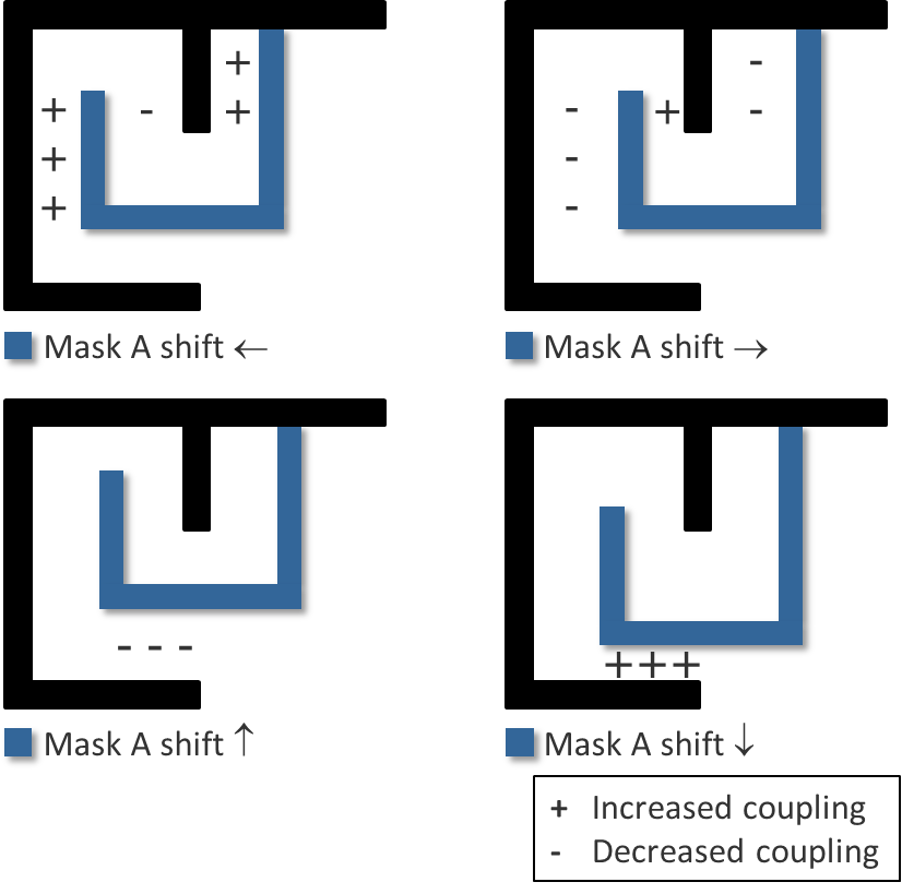
Figure 3. Mask 1 will have some misalignment with Mask 2. Depending on whether Mask 2 shifts to the left, right, up, or down, the coupling capacitance will increase or decrease.
To accurately model these shifts, it is necessary to have tables for modeling optical process corrections (OPC), bias, and thickness variation that are color-aware (Figure 4).
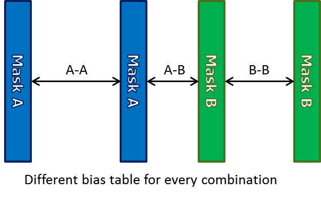
Figure 4. With a double patterned layout, there must be bias tables that allow for every possible color assignment.
Advanced extraction tools like the Calibre xACT parasitic extraction tool provide full extraction support for multi-patterned designs, including both colored and uncolored layouts.
In addition to the process corners due to variations in metal and dielectric thicknesses, the Calibre xACT tool also produces netlists with double patterning corners to feed into accurate signal integrity analysis.
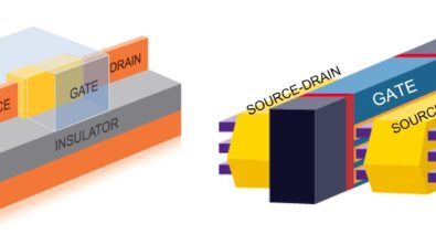
FinFETs
Starting at 16/14 nm, and moving into 10 nm, finFETs are used as the device of choice. FinFETs have a lower threshold voltage than planar CMOS, which means that a lower supply voltage can be used, making them extremely desirable for low power design.
The job of modeling finFETs is split between the device model and the parasitic extraction tool. The foundry developing the design kit determines which parasitic effects go into the device model, and which effects should be extracted by the parasitic extraction tool (Figure 5).
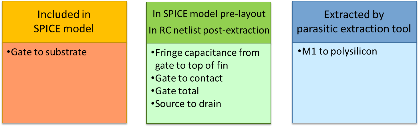
Figure 5. Foundries decide how and when finFET capacitances are managed.
One common device model for finFETs is the BSIM-CMG model. BSIM-CMG uses an ideal single fin model, and there are minimal layout-dependent effects.
One of the challenges of modeling layout-dependent effects is that 3D effects are quite significant, and difficult to reduce to a model. Also, devising an effective profile to be used in extraction is a challenging task.
While some of the capacitances that exist in finFETs can be modeled in the device model, they are often more accurately characterized by the extraction tool. Such effects can be included in the pre-layout simulation, but turned off in the device model post-extraction.
For example, the parasitic extraction tool can determine local interconnect width, gate width, fin count, fin spacing, and gate-to-local interconnect spacing, and can therefore calculate an accurate total gate capacitance value in the post-extraction simulation stage.
There are other effects that can only be captured by the parasitic extraction tool, such as coupling capacitance to Metal1. To accommodate this division of responsibilities, the Calibre xACT tool enables designers to include or exclude certain parasitic effects, ensuring that there is no double counting, or missed effects.
Parasitic Resistance Extraction
Accurate parasitic resistance extraction is very important for low power design, because of the need for accurate electromigration and IR drop analysis. Simulation flows for both of these require accurate resistance values, as well as accurate reported widths. The metal width’s nominal value starts as the drawn width of the polygon, but then is altered, due to lithography effects (Figure 6).
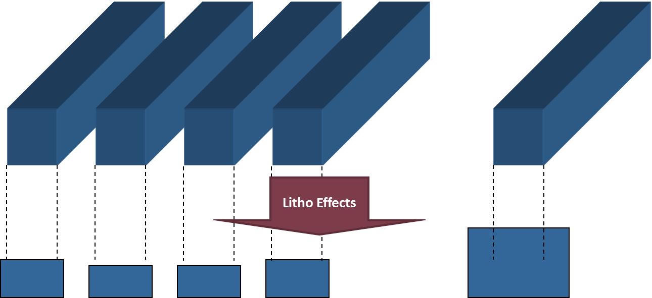
Figure 6. Lithography effects change the width of polygons.
When the metal is thinner than designed, parasitic resistance is higher. For IR drop, this means the voltage drop across these narrowed interconnect polygons will be higher. For electromigration analysis, the current density will be higher, because the interconnect is narrower. The Calibre xACT tool not only accurately extracts parasitic resistance, but outputs actual width values that take lithography effects into consideration.
Post-Extraction Analysis
After extraction, a netlist is created (for example, in DSPF format). SI analysis can then be performed. If SI issues are identified, the layout must be modified.
For example, if there is too much crosstalk between two lines, those lines must be moved further apart. If the current density is too high in a certain area, or if the IR drop is too high, the metal must be widened to reduce the parasitic resistance. A viewing environment like the Calibre RVE™ tool can be used to visualize where parasitics are too high (Figure 7).
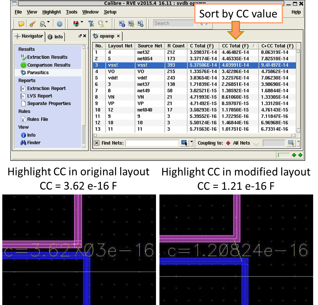
Figure 7. Using a results viewing environment to display parasitic results can help pinpoint their layout location, enabling faster and more accurate corrections. Moving the two wires farther apart reduces their coupling capacitance, which reduces crosstalk issues.
At advanced nodes, designers must be aware of new and magnified parasitic effects that can affect the performance, manufacturability, and power consumption of their designs.
Parasitic extraction tools that help designers identify and resolve these concerns accurately and efficiently ensure these designs can reach production in a timely and profitable manner.
Have you seen signal integrity issues while moving to advanced nodes? How have you overcome these issues?
Author
Karen Chow is a Technical Marketing Engineer in the Design-to-Silicon division of Mentor Graphics Corp., focusing on driving parasitic extraction development in analog and RF design flows.

This article was originally published on www.eetimes.com