Electrical Overstress Detection and Debugging
By Dina Medhat, Mentor Graphics
Automated voltage propagation provides an accurate way to detect and correct those hard-to-find EOS conditions early in the verification flow.

Electrical overstress (EOS) is one of the leading causes of integrated circuit (IC) failures, regardless of where the chip is manufactured. EOS events can result in a wide spectrum of outcomes, from no damage, to degrees of performance degradation, up to catastrophic damage where the IC is permanently non-functional. Identifying and removing EOS susceptibility from integrated circuit (IC) designs is essential to ensuring successful performance and reliability when the products reach the market.
EOS in its broadest definition includes electrostatic discharge (ESD) events. However, these two effects are generally differentiated, with EOS being more narrowly defined as the occurrence of overvoltage or overcurrent to a device. For comparison, let’s look at the significant properties that separate EOS and ESD definitions in the IC industry (Table 1) [1] [2].:
With these differences in mind, we’ll use EOS to describe the thermal damage that may occur when an electronic device is subjected to a current or voltage that is beyond the specification limits of the device. This thermal damage is the result of the excessive heat generated during the EOS event, which in turn is a result of resistive heating in the connections within the device. The high currents experienced during the EOS event can generate very localized high temperatures, even in the normally low resistance paths. These high temperatures cause destructive damage to the materials used in the device’s construction [3].
As shown in Figure 1, EOS damage can be external (visible to the naked eye or with a low-power microscope), or internal (visible after decapsulation with a high-power microscope). External damage can include visible bulges in the mold compound, physical holes in the mold compound, burnt/discolored mold compound, or a cracked package. Internal damage manifests itself in melted or burnt metal, carbonized mold compound, signs of heat damage to metal lines, and melted or vaporized bond wires.
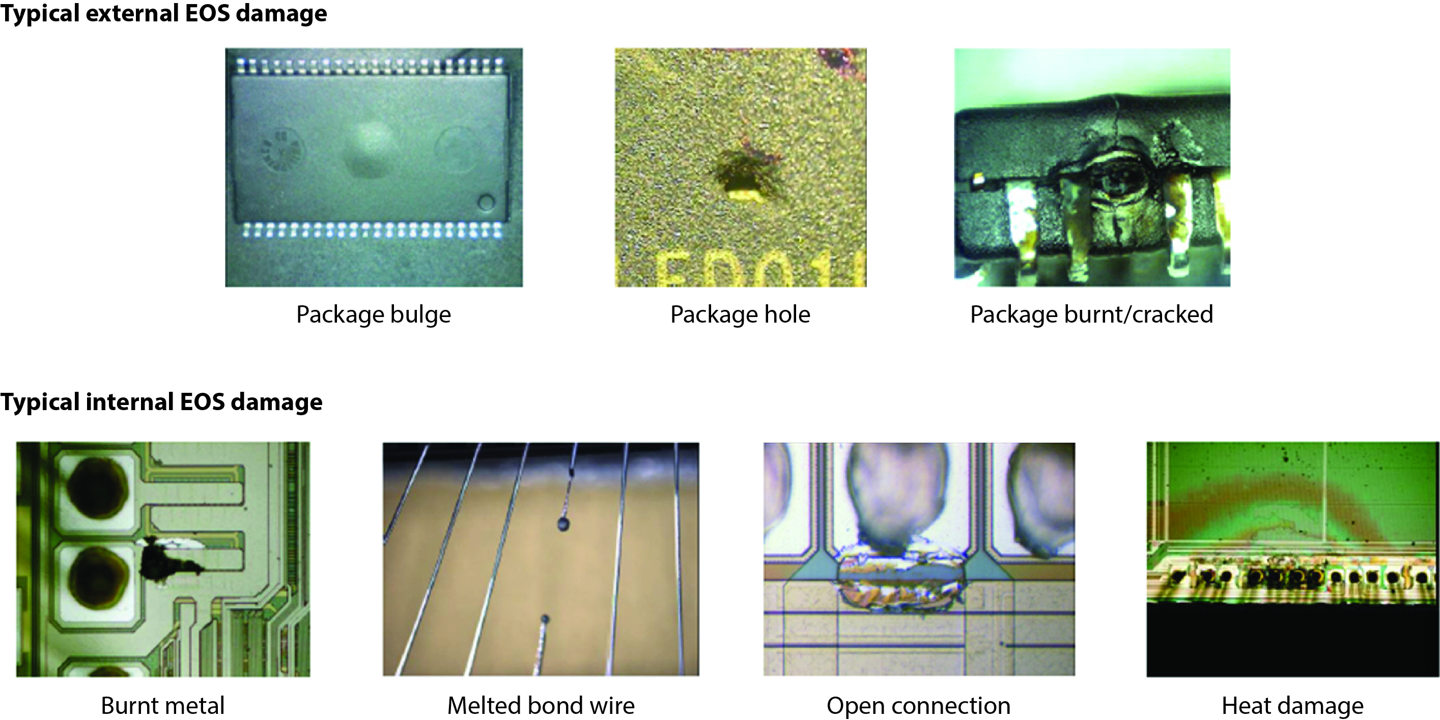
Figure 1: Examples of external and internal EOS damage [3]
Obviously, preventing EOS conditions is a good idea! To do that, designers must check for overvoltage conditions on devices during verification. In the past, designers have used a variety of methods, relying mainly on the expertise of the design team. Manual inspection is probably the most tedious and time-consuming approach, and hardly practical for today’s large, complex designs. Another conventional approach is the use of design rule checks (DRC) in combination with manually-applied marker layers. Adding marker layers is inherently susceptible to mistakes and forgetfulness, and this approach also requires additional DRC runs, extending verification time. Lastly, there is simulation, which can also take a long time to run, and is dependent on the quality of the extracted SPICE netlist, SPICE models, stress models, and input stimuli.
We should also note that EOS risk is not necessarily highest in advanced node designs. While the smaller devices, thinner wires, and thinner gate oxides of these nodes are more susceptible to EOS, legacy technology faces its own unique challenges as designs are re-engineered for new high-reliability, environmentally-demanding applications, such as automotive and medical. In addition to new stresses and longevity requirements, there are new circuit functions and topologies that were not present in the first designs of a legacy node. Increased analog content, higher voltages, and higher frequencies are just a few of the new design challenges that add new constraints on designs originally implemented in more mature process nodes.
With these new constraints and requirements comes the need for new verification techniques that can efficiently analyze designs and find potential EOS failure points and susceptibility. At Mentor Graphics, we addressed advanced EOS reliability checking [4] [5] by developing a new automated functionality known as voltage propagation. Using the Calibre® PERC™ tool to run voltage propagation [Figure 2] enables designers to perform an efficient, automated static analysis on large designs. The basic functionality of voltage propagation is simple: you define voltages (at a minimum, on supplies), then define rules to propagate them to internal nodes in a static way to catch violations. This functionality is both powerful and flexible, because you can define advanced propagation rules based on your design needs. From a debugging perspective, you can use the Calibre RVE tool to interactively trace voltages, giving you a better understanding of how they were propagated on your design, which enables you to debug errors more quickly and efficiently.
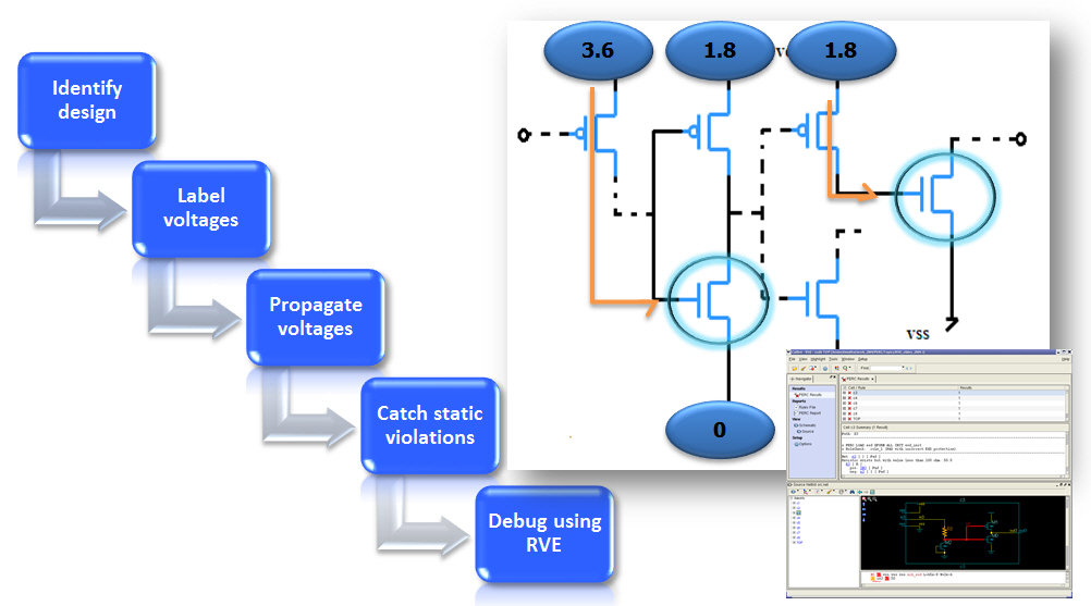
Figure 2: Calibre PERC can assign voltages to all internal nodes of the SOC in an efficient static way
To show you the process, let’s debug a typical over-voltage (EOS) condition. As you can see in Figure 3, the Calibre PERC run identifies a device with a 3.3V difference between propagated voltages to gate pin and source pin, which is greater than the allowed breakdown limit of 1.8V for this device type. To debug this violation, you first highlight the violating device in your schematic viewer. Next, you must understand how the gate can receive a propagated voltage of 3.3V. To do that, you ask Calibre RVE to trace the gate pin. This trace results in the details of the voltage propagation paths being shown in the voltage trace window (where “start” is the gate pin and “break” is the 3.3V net). You can then click on specific devices/nets from the voltage trace window to highlight them in your design data in the schematic viewer, providing you with the information you need to analyze and resolve the voltage overload condition.
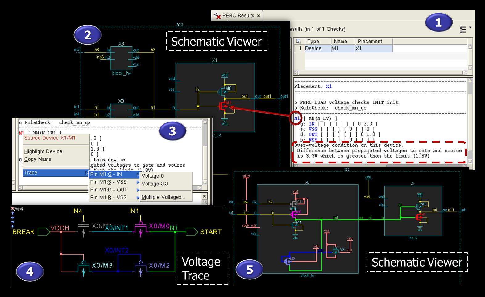
Figure 3: Calibre PERC: Voltage Propagation Interactive Debugging
Designers at both advanced and legacy nodes are facing new and expanded reliability demands as designs are developed and re-engineered for new applications. New functionality such as automated voltage propagation can provide the fast, accurate identification of EOS conditions in a design, enabling designers to analyze and correct the design early in the verification flow. Finding and eliminating these often-subtle susceptibilities helps ensure that these designs will satisfy the performance and reliability expectations of the market.
References:
[1] https://en.wikipedia.org/wiki/Failure_modes_of_electronics
[2] http://www.bestesd.com/library/Origins-of-EOS.pdf
[3] http://www.cypress.com/file/97816/download
[4] Lescot, J.; Bligny. V.; Medhat, D.; et.al. “Static Low Power Verification at Transistor Level for SoC Design” International Symposium on Low Power Electronics and Design (ISLPED) 2012, July 2012.
[5] http://www.mentor.com/products/ic_nanometer_design/verification-signoff/circuit-verification/calibre-perc/
Author
Dina Medhat is a technical lead for Calibre Design Solutions at Mentor Graphics. She has been with Mentor Graphics for ten years in various product and technical marketing roles. She holds a BS and an MS from Ain Shames University in Cairo, Egypt.

Liked this article? Then try this –
How-To Video: Checking for electrical overstress using Calibre PERC
White Paper: Improving Design Reliability by Avoiding Electrical Overstress
This article was originally published on www.eetimes.com


