Sign-off lithography simulation and multi-patterning must play well together
By Joe Kwan, Mentor Graphics
At 20 nm and below, designers must ensure their lithography simulation can incorporate and analyze multi-patterning requirements and effects to ensure lithographic fidelity
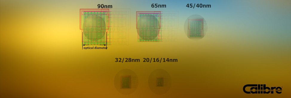
By now if you haven’t heard about the challenges of manufacturing at ever-shrinking process nodes, you must be living in a silicon cave. Since the 90 nm process node, manufacturers have been using 193 nm lithography. As process nodes advanced from 90 to 65 to 45 to 28, and now to 20 and 16 nm, the corresponding transistor sizes and interconnects shrunk as well. However, the light source has remained at 193 nm (Figure 1).

Figure 1. Transistor and interconnect sizes have decreased dramatically, while available lithography light sources have remained the same.
High fidelity silicon manufacturing at process node shrinks with ever deeper sub-wavelength features is akin to painting a thin, extremely precise line using a very wide brush. During lithography, the contoured shapes of the actual silicon printed on the chip are not the same as the perfectly rectilinear shapes drawn by design tools. The shapes of the contours vary depending on such factors as process conditions and the lithographic influence of neighboring geometries. What you draw is not exactly what you get (Figure 2).
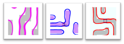
Figure 2. Lithographic results approximate the drawn geometries.
The EDA industry first introduced a number of technologies to sustain successful lithographic resolution. These included simple rule-based optical process correction (OPC), model-based OPC, and sub-resolution assist features (SRAF). Foundries applied them to a design after tapeout. But at 65/45nm, it became apparent that lithographic variation could no longer be fully addressed post-tapeout using OPC.
This led to the introduction of early lithographic simulation during the intellectual property (IP) and chip design phases. This generation of tools has been commonly grouped together under the concept of ‘litho-friendly design’ (LFD). LFD allows design teams to find and correct lithographic ‘hotspots’ before tapeout.
Lithography with multi-patterning
However from 20nm, another generation of enabling technology has become necessary. Design features are now so small and the designs themselves so tightly spaced that bringing them together in a single lithographic resolution has become impossible. Double patterning has therefore already become mandatory to enable design production at 20nm. Below that, foundries are evaluating other multi-patterning strategies (e.g., triple and quadruple patterning).
Multi-patterning ‘splits’ the layout into two or more separate masks. This allows foundries to image a design using separate exposures for each mask while still drawing upon established OPC solutions (Figure 3). By splitting a layer onto multiple masks, manufacturers can squeeze more and finer geometries into a smaller space.

Figure 3. Possible multi-patterning mask assignments
However, multi-patterning imposes new requirements on the designer in terms of layout, physical verification, and debug. Multiple decomposition solutions exist for any one layout, and debugging corrections may also have multiple adjustment options. As well as checking these new multi-patterning design rules, the designer must still perform sign-off lithography verification. The lithography simulator must accept multi-patterned designs, or be able to perform production multi-patterning decomposition.
Moreover, multi-patterning potentially leads to additional variation due to the overlay (misalignment) of the merged masks. Depending on alignment of the masks, you may see pinching hotspots (narrowing of wires) or bridging hotspots (not enough space). So, a lithography verification tool must be able to analyze not only the geometries on the same color mask, but also the different color masks of the merged contours (Figure 4).

Figure 4. Simulations must analyze both a single color mask and the merged results of multiple masks to identify all potential hotspots
Lithography sign-off must be production-accurate to precisely identify hotspots and weak patterns in the verification flow. Just as a lithography simulator must include an exact copy of production OPC techniques, it must also incorporate production-accurate multi-patterning requirements.
To ensure full and accurate coverage, sign-off lithography verification must be able to support:
- accurate multi-patterning decomposition;
- lithographic contour simulation of individual masks;
- checks of individual mask simulation results; and
- checks of the contours on merged masks to account for overlay alignment.
Introducing multi-patterning requirements into the design and verification flow is causing a major shift in the responsibilities facing design teams. Unless and until new technology arrives to replace 193nm scanners, you must have the tools and technologies to verify the lithographic fidelity of multi-patterned designs to achieve timely tapeouts and success in manufacturing.
Author
Joe Kwan is the Product Marketing Manager for Calibre LFD and Calibre DFM Services at Mentor Graphics. He previously worked at VLSI Technology, COMPASS Design Automation, and Virtual Silicon. Joe received a BA in Computer Science from the University of California, Berkeley, and an MS in Electrical Engineering from Stanford University. He can be reached at joe_kwan@mentor.com.
This article was originally published in www.techdesignforums.com