The Route to Faster Physical Verification and Better Designs
By Nancy Nguyen and Jean-Marie Brunet, Mentor Graphics
Using the most accurate and up-to-date signoff engine instead of a limited P&R tech file is essential when routing at advanced nodes.

As we’ve moved to today’s leading-edge nodes, physical layout designers have faced more and more challenges to get their design to tape-out on schedule. Timing becomes increasingly difficult to converge, power reduction for both IR and leakage becomes a big issue, and most importantly, how do we meet all of the ever-growing and more complex signoff design requirements? In this article, we’ll look at the challenges of meeting sign-off design rules—these challenges exist even for a “mature” advanced node like 28 nm and the challenges continue to grow with each new process node.
As processes shrink with every node advance, printability is becoming a major issue. Low printability affects yield, which in-turn affects cost and profitability. In the course of improving printability, foundries identify sets of problematic layout patterns that cause low printability in their processes, starting from 28 nm. These problematic patterns vary with different foundries and different process nodes. Because the problematic patterns are unique to each foundry, rules for identifying these patterns are coded and encrypted in the foundry’s signoff design rule checking (DRC), pattern matching (PM) and Litho Friendly Design (LFD) decks—they are not exposed to the layout designers. The challenge the layout designers face is how to ensure the layout is clean of these problematic patterns without knowing what these patterns look like.
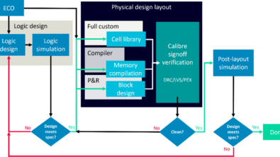
If we look at the conventional physical design flow, the layout designers depend heavily on the place and route (P&R) tool, which uses the rules defined in a P&R tech file (a limited subset of the full signoff DRC deck) to create a layout that is presumptively DRC-clean. Once the layout is P&R tech file clean, the layout is verified with the foundry signoff DRC/PM/LFD decks, using the physical verification tool (Figure 1). In most cases, if the foundry rules are clearly described in the design rule manual, EDA tool companies can enhance their P&R tech file to accommodate the new and expanded rules for each new node.
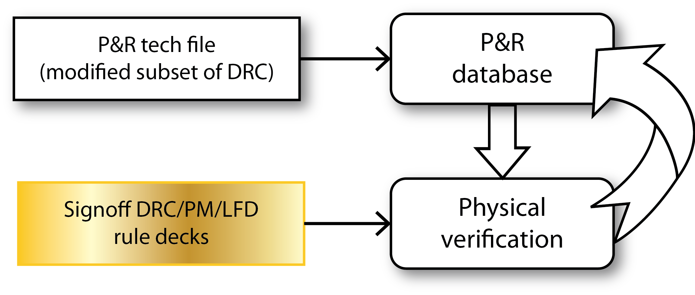
Figure 1. Traditional P&R physical verification uses the P&R tech file during routing, then sends the routed layout through a full signoff DRC/PM/LFD run to ensure the layout is completely DRC-compliant.
However, for problematic patterns that are encoded and encrypted, the only tool that can capture these patterns correctly is the physical verification tool that uses the foundry signoff DRC, PM and LFD decks. Because these patterns are not exposed to the P&R tool through the P&R tech file, it is not uncommon for routers to unwittingly generate these patterns during the place and route process, only to have them appear as errors in the full signoff DRC/PM/LFD verification run. This limitation raises the complexity of both error detection and fixing for the layout designers because they can no longer rely on the P&R tool to get the layout predominantly clean for final verification and tapeout.
Until recently, the only real fix available to designers was to instruct the router to rip up and re-route the areas containing the problematic patterns. However, this was a game of chance—the designers had to hope that the router did not unknowingly create another problematic pattern during the re-route. The rip up and re-route approach usually requires multiple full-block validation runs to get to DRC-clean, each adding to overall runtime. In addition, because a significant portion of the design’s routing may change, the timing may be affected, which would require additional time for timing closure.
A new, less disruptive, and far more efficient approach is now available that uses a technique known as Local Layout Manipulation. It uses an integrated tool solution during the P&R process that accesses the full signoff DRC/PM/LFD deck for pattern recognition and analysis, and contains built-in intelligence for analyzing the encrypted problematic pattern definitions supplied by the foundries (Figure 2).
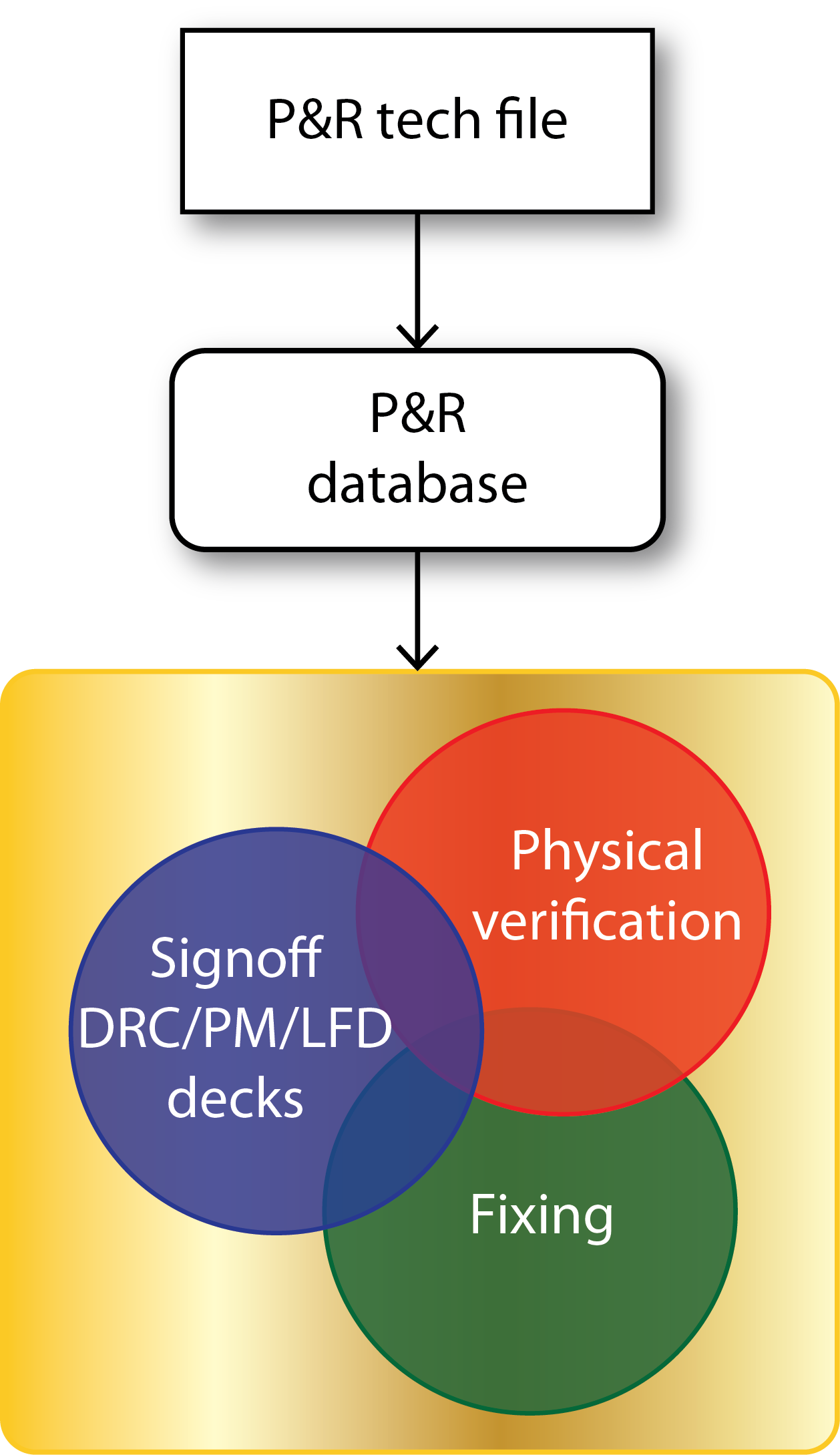
Figure 2. Local Layout Manipulation allows the router to access signoff DRC/PM/LFD decks during fixing to eliminate and avoid creating new problematic patterns.
By accessing the most accurate and up-to-date signoff DRC/PM/LFD engine in place of the limited P&R tech file when verifying routing, this solution ensures that problematic patterns are efficiently replaced and no additional problematic patterns are created during the fixing process. In addition, because the Local Layout Manipulation process is threaded, multiple problematic pattern issues can be resolved simultaneously during fixing, reducing the time required to achieve a DRC/PM/LFD-clean design. With Local Layout Manipulation, layout designers now have the ability to repair the layout without multiple time-consuming DRC/PM/LFD verification runs, and with minimal impact on timing and the overall design.
Authors
Nancy Nguyen is a Product Lead for Design for Manufacturing (DFM) and Place and Route Integration in the Design-to-Silicon division of Mentor Graphics. Using her comprehensive understanding of the manufacturing/verification closure challenges encountered at advanced nodes, Nancy focuses on the development of products that analyze and modify the layout to improve the robustness and quality of the design. Prior to Mentor Graphics, Nancy worked at Chartered Semiconductor, Intel, Cisco, and LSI. Her experience includes physical design implementation, chip integration, and physical design methodology development for new technology nodes, including power planning and power optimization. Nancy holds a BS degree in Computer Engineering from USC. She can be reached at nancy_nguyen@mentor.com.
Jean-Marie Brunet is the Product Marketing Director for Design for Manufacturing (DFM) and Place-and-Route Integration at Mentor Graphics Corporation. He has served in application engineering, marketing and management roles in the EDA industry, and has held IC design and design management positions at STMicrolectronics, Cadence, and Micron among others. His experience includes working with pure-play foundries to resolve complex yield issues related to OPC and RET. Jean-Marie holds a Master’s degree in Electrical Engineering from I.S.E.N Electronic Engineering School in Lille, France. Jean-Marie Brunet can be reached at jm_brunet@mentor.com.
This article was originally published in www.seminengineering.com