Part 3: The 2018 Wilson Research Group Functional Verification Study
This blog is a continuation of a series of blogs related to the 2018 Wilson Research Group Functional Verification Study (click here). In my previous blog (click here), I presented the findings from our new study related to how successful FPGA projects are in terms of verification effectiveness. In this blog I focus on FPGA verification effort trends.
FPGA Verification Effort Trends
Directly asking study participants how much effort they spend in verification will not work. The reason is that it’s hard to find a paper or article on verification that doesn’t start with the phrase: “Seventy percent of a project’s effort is spent in verification…” In other words, the industry is already biased to respond with this effort value. Yet, there are really no creditable references to quantify this value.
I don’t believe that there is a simple answer to the question, “How much effort was spent on verification in your last project?” In fact, I believe that it is necessary to look at multiple data points derived from multiple questions to truly get a sense of effort spent in verification. And that’s what we did in our functional verification study.
Percentage of Project Time Spent in Verification
To try to assess the effort spent in verification, let’s begin by looking at one data point, which is the total project time spent in verification, as shown in Fig. 3-1. You can see two extremes in this graph. In general, projects that spend very little time in verification are typically working on designs with a good deal of existing pre-verified design IP, which is integrated to create a new product. On the other extreme, projects that spend a significant amount of time in verification often have a high percentage of newly developed design IP that must be verified.
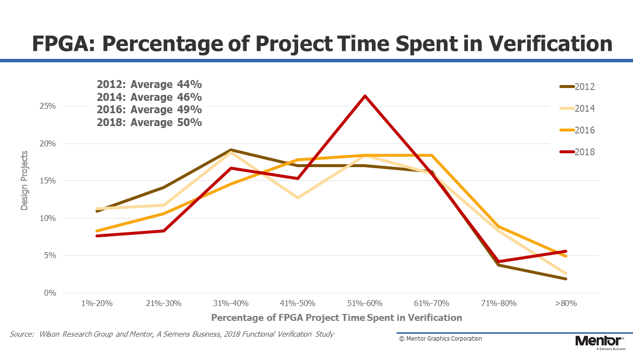
Figure 3-1. Percentage of FPGA project time spent in verification
Overall, we found an increase in average percentage of FPGA project time spent in verification during the period 2014 through 2018. Again, this is an indication of growing design and verification complexity.
Peak Number of Design and Verification Engineers
Perhaps one of the biggest challenges today is to control cost and engineering headcount, which means identifying FPGA design and verification solutions that increase productivity. To illustrate the need for productivity improvement, we discuss the trend in terms of increasing engineering headcount. Fig. 3-2 shows the mean peak number of FPGA engineers working on a project.
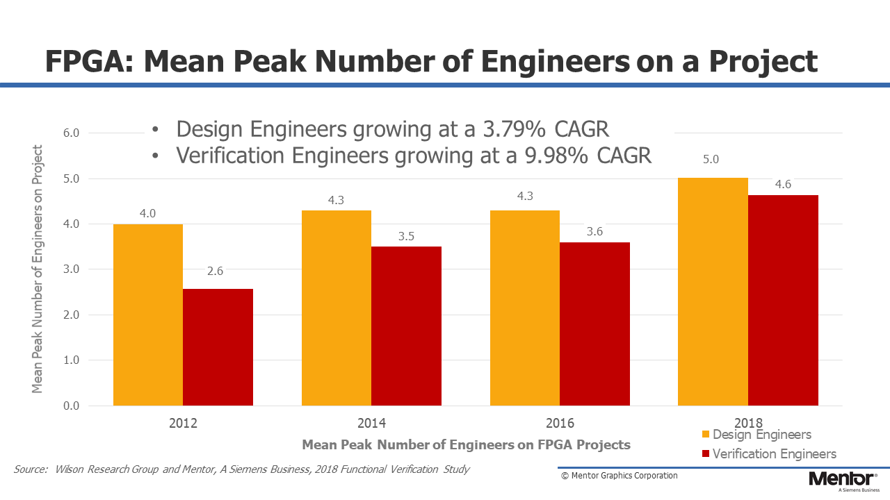
Figure 3-2. Mean Peak Number of FPGA Engineers Working on a Project
While, on average, the demand for design engineers is growing at about a 4% CAGR (which is similar growth for IC/ASIC), the demand for verification engineers is growing at about a 10% CAGR. It is worth noting that during the period 2007 through 2014, the IC/ASIC market went through similar growth demands related to verification engineers to address growing verification complexity.
In my next blog (click here) I focus on the time that FPGA design and verification engineers spend in various task.
Quick links to the 2018 Wilson Research Group Study results
- Prologue: The 2018 Wilson Research Group Functional Verification Study
- Understanding and Minimizing Study Bias (2018 Study)
- Part 1 – FPGA Design Trends
- Part 2 – FPGA Verification Effectiveness Trends
- Part 3 – FPGA Verification Effort Trends
- Part 4 – FPGA Verification Effort Trends (Continued)
- Part 5 – FPGA Verification Technology Adoption Trends
- Part 6 – FPGA Verification Language and Library Adoption Trends
- Part 7 – IC/ASIC Design Trends
- Part 8 – IC/ASIC Resource Trends
- Part 9 – IC/ASIC Verification Technology Adoption Trends
- Part 10 – IC/ASIC Language and Library Adoption Trends
- Part 11 – IC/ASIC Power Management Trends
- Part 12 – IC/ASIC Verification Results Trends
- Conclusion: The 2018 Wilson Research Group Functional


Comments