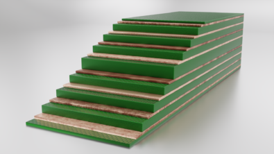
What are the advantages and disadvantages of a thinner PCB?
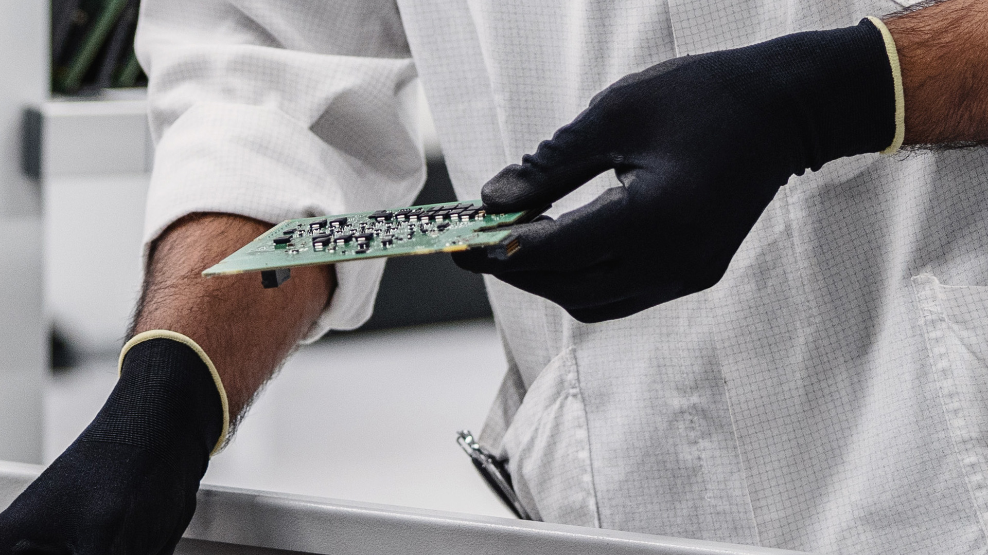
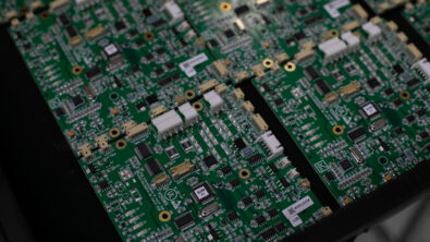
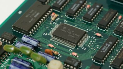
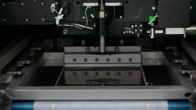
Design for manufacturing (DFM) is an essential aspect of the new product introduction (NPI) process, and PCB design is a critical component of DFM. PCB design can have a significant impact on the manufacturing process, and designers must consider a wide range of factors when developing PCB stack-up design. One such factor is the thickness of the PCB, which can have both advantages and disadvantages for the manufacturing process. The printed circuit board (PCB) is also a crucial component in itself as part of the electronic device, and its thickness plays a significant role in determining the overall performance and functionality of the device. In this blog, we will discuss the advantages and disadvantages of a thinner PCB.
Advantages of Thinner PCBs:
- Improved Signal Integrity: Thinner PCBs can offer improved signal integrity, which can be critical in high-speed or high-frequency applications. This is because thinner PCBs have lower capacitance and inductance, resulting in better signal transmission and reduced signal loss.
- Reduced Cost: Thinner PCBs require less material, which can lead to cost savings in both material and manufacturing. Additionally, thinner PCBs may require less drilling and routing, which can further reduce manufacturing costs.
- Reduced weight: A thinner PCB weighs less, which makes it ideal for portable electronic devices such as smartphones, laptops, and tablets. This is especially important for devices that need to be carried around frequently, as a lighter device will be more comfortable to hold and transport.
- Reduced space: A thinner PCB takes up less space, which is important for devices that need to be compact and portable. This is particularly useful for devices that need to be integrated into tight spaces, such as laptops, tablets, and smartphones.
- Improved thermal management: A thinner PCB can provide better thermal management by dissipating heat more efficiently. This is particularly important for devices that generate a lot of heat, such as high-performance CPUs and GPUs.
- Increased Flexibility: Thinner PCBs are more flexible and can be used in applications where space is limited or where the board needs to be flexible. This can be especially useful in applications such as wearables, medical devices, or aerospace applications.
Disadvantages of Thinner PCBs:
- Increased susceptibility to external factors: A thinner PCB is more susceptible to external factors such as humidity, temperature, and vibration. This can lead to increased corrosion and damage, which can negatively impact the overall performance and lifespan of the device.
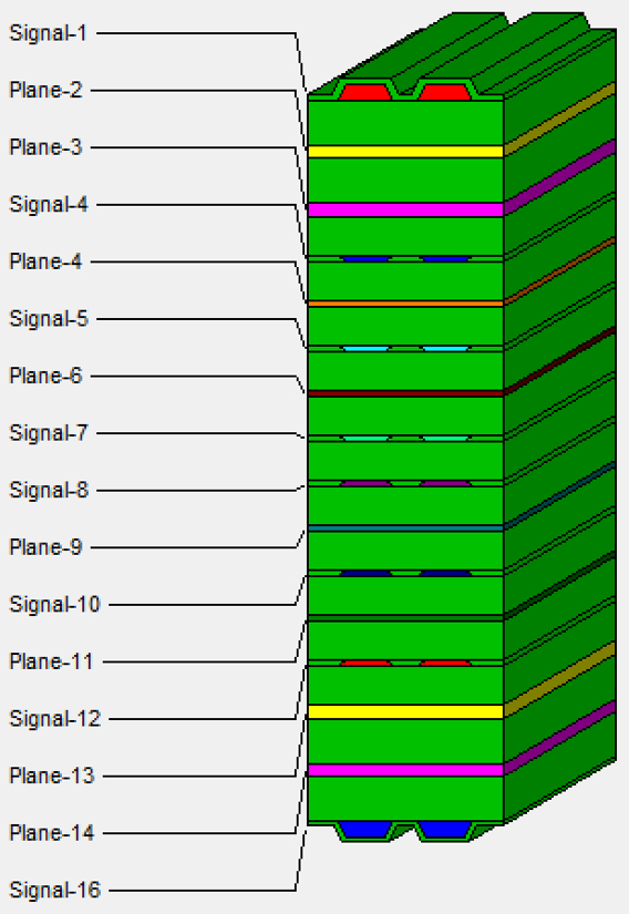
- Limited Layer Count: Thinner PCBs may have limitations on the number of layers that can be used, which can limit the complexity of the design. This can be a significant disadvantage in applications where the design requires a high number of layers or complex routing.
- Reduced Durability: Thinner PCBs are more fragile and can be more susceptible to damage during handling or assembly. This can lead to manufacturing defects or a shorter lifespan of the final product.
- Increased Risk of Warping: Thinner PCBs can be more prone to warping during the manufacturing process, which can cause issues with assembly or result in a final product that does not meet specifications.
- Reduced mechanical strength: A thinner PCB is less durable than a thicker one, which makes it more prone to damage. This can be a major drawback for devices that are subjected to high levels of stress, such as wearables and portable medical devices.
- Reduced signal integrity: Thinner PCBs can be a bit more challenging as there is less vertical distance to work with to create a proper stack up. The necessary layer to layer spacings of a thinner PCB causes increased crosstalk and signal loss, which can negatively impact the overall performance of the device. This makes is especially important to develop a proper stack up plan.
- Reduced current carrying capacity: A thinner PCB can have reduced current carrying capacity, which can be a drawback for devices that require high current levels.
- Difficult to assemble: A thinner PCB can be more difficult to assemble than a thicker one, as it requires more precision and care during the assembly process. This can lead to increased manufacturing costs and longer production times.
Manufacturing Driven Design and the Role of Valor NPI:
Manufacturing driven design is a critical aspect of DFM, and it involves designing products that are optimized for manufacturing. This includes considering factors such as material selection, assembly, and testing requirements, as well as the impact of the design on the overall manufacturing process.
Valor NPI is a software solution that can be used to support manufacturing driven design. It includes a range of tools and features that can be used to optimize the PCB design for manufacturing, including PCB stackup design, manufacturing analysis, and design verification.
One of the key advantages of Valor NPI is its ability to optimize the PCB stackup design for manufacturing. This includes considering factors such as the thickness of the PCB, the number of layers, and the placement of components, in order to create a design that is both functional and manufacturable.
Additionally, Valor NPI includes a range of manufacturing analysis tools that can be used to identify potential issues with the design, such as manufacturing defects or assembly problems. This can help designers to identify and address these issues early in the design process, reducing the risk of costly rework or delays during manufacturing.
In conclusion, a thinner PCB offers several advantages such as reduced weight, space, and cost. However, it also has its share of disadvantages such as reduced mechanical strength, signal integrity, and current carrying capacity. Therefore, the decision to use a thinner PCB should be based on a careful analysis of the specific requirements of the device and the trade-offs involved.