What is DFM and DFA?
Basically, the acronym DFM stands for “Design for Manufacturing” while DFA translates to “Design for Assembly“. To further clarify the difference between them is in their particular focus. However similarly they both are purposed to make product design easy to manufacture. Where DFM focuses in the area that will make individual components easy to get or cost-efficient to manufacture. While DFA focuses on how to improve the assembly of such components to improve the cost-efficiency of developing the product.
Because there are so many aspects and decisions involved related to both Design for Manufacturing and Design for Assembly it would be impossible to address all possibilities in this brief blog. DFM and DFA are relevant to almost any product be it assembling bicycles where primarily the product is mechanical components to electronic devices such as cell phones, routers, and computers which require both mechanical and electrical components. The primary focus of this blog will be PCB Design through PCB Fabrication and PCB Assembly within the electronic realm and how it relates to DFM and DFA.
I tend to look at a more granular level where DFM is the catalyst to improve the PCB Design layout improving the fabrication of the Printed Circuit board such as line widths, PCB stackups, use of standard materials, technology types, etc. An integral part of making the product more manufacturable is in keeping the process as simple as possible to achieve the desired end goal. One example would be the initial decision process made in advance as to technology type, will blind and buried vias be required when a standard through hole design can get the job done. Will the design require microvias or even a VIPPO (via in pad) approach? All of these early decisions as you begin the design will drastically affect its manufacturability and cost throughout the process.
Where I tend to look at DFA as the means to improve the component assembly process. One example of this would be by providing proper component spacing to allow for proper assembly or access to components for rework and test. This is best achieved when you have accurate component information and sizes along with pin contact area to assure you have a proper pin to pad size relationship for good solderability. Of course, this is best achieved when you have the ability to import your Bill of Material (BOM) directly into your design along with alternate parts to verify the proper spacings, height concerns and perform a true solderability analysis of your design.
Having worked in the OEM world for over 30 plus years managing a number of PCB Design teams at a number of large companies, I have found it is imperative to work closely with your PCB Fabricators and Assembly houses to optimize your designs for manufacturability and assembly. I’ve gotten to understand the concept that “It’s possible to manufacture most things that are designed… If there is enough time, money, and resources” However, its more cost effective to design quality and efficient manufacturing practices into the product from its inception, accomplishing this means:
Abandon the old Design/Manufacturing paradigms such as:
- Over the wall: The old tradition methodology, which utilizes little to no communication between design and manufacturing
- Improve the communications and collaboration between the Design team and manufacturing for critical information
- Sign-off: Where manufacturing documents are approved and signed off by manufacturing after the fact
Adopt shift left Concurrent Engineering approach:
- Design philosophy that requires that all stake holders such as Design Engineers, Component Engineers, PCB Designers, Test Engineers, MFG Engineers and PCB Fabrication experts engage in the design-decision making process.
- Design Engineers typically are experts in design but not manufacturing, test, board fabrication or assembly. Make sure you get expertise in those areas as part of the decision-making process.
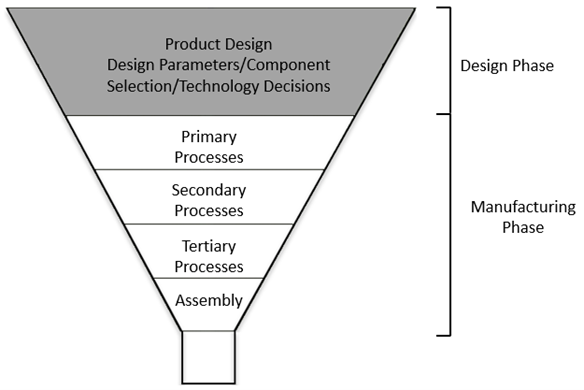
- Rule of thumb is 60% – 80% of a product cost is determined by design decisions so address these manufacturing issues as early as possible in the product development process. I like to think of this as the funnel approach as the product moves through the product development cycle the opportunity for manufacturing improvements get restricted. Do your homework early and get your stake holders involved in the design stage, don’t wait to make important decisions at a later date when the cost of that change goes up exponentially.