Video: Developing DFT flow for 3D IC at Broadcom
At the 2023 North America User2user symposium, Broadcom master engineer Saket Goyal discussed his team’s experience using Tessent Multi-die software to build a test flow for their 3D chips. The session was recorded and is now available for anyone to view.
Goyal, who is a principal leader in the ASIC products division, describes how Tessent provided real solutions for their ASIC products.
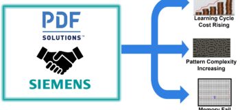
Goyal’s team needed a tool and flow for ASIC products that met the DFT challenges they face today, including effects of technology scaling, IP integration, packaging, low power, time-to-market, ramp to production, and system scaling.
For 3D IC designs, there are specific test challenges, which Goyal goes over. He then covers the requirements for Broadcom ASIC products and the long list of Tessent solutions for 3D IC.
Given all the challenges, the first and foremost issue is how to get access to each die, each DFT structure in each die, from the package level.
Saket Goyal, Broadcom
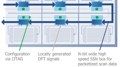
To solve the die access problem, Broadcom has adopted the IEEE 1838 standard describes the test access architecture for such 3D stacked devices and describes the required serial access mechanism using Primary Test Access Port (PTAP) or Secondary Test Access Port (STAP). Broadcom also uses the Flexible Parallel Port (FPP) access mechanism to deliver volumes of scan patterns.
Goyal walks us through some components of the Broadcom 3D IC architecture, including the PTAP and STAP. Re-use of the TAP as a PTAP is accomplished with Tessent Multi-die software. He also talks about the die wrapper register (DWR) and test modes that allows die-to-die interfaces. This was built with minor changes from their existing Tessent hierarchical DFT flow. The FPP was implemented using Tessent SSN, the bus-based packetized test solution.
In summary, Broadcom was able to extend their Tessent hierarchical DFT methodology to include the 3D stack by introducing IEEE 1838. They limited the internal scan architecture to tradition EDT and used Tessent SSN for inter-die packetized scan data delivery. The Tessent Multi-die product has enabled key changes in existing DFT flow while reusing a majority of IP to support their 3D IC test challenges and speed up time-to-market.