Ensure IC quality with Tessent

Quality, reliability safety and security are key considerations when designing ICs but not all chips and systems are designed equal. However, if you are designing SoCs for automotive, aerospace or medical, then the process of designing, manufacturing, testing, and in-life monitoring becomes much more difficult. The challenges range from adherence to standards and regulations, managing capital investments and engineering resources, securing the right tools and flows, and establishing methods to manage the vast amounts of data that inform each step in the lifecycle of the device. Tessent solutions help you ensure high SoC quality, enhance safety, optimize security and increase reliability so you can get your product to market faster.
Today, let’s talk about how Tessent boosts the semiconductor quality.
Why focus on IC quality
IC quality is made up of a number of parts; how well a chip functions, how reliable it is, how safe and secure it is and even how thoroughly tested it is for physical defects and potential latent or future defects. Quality affects the bottom line: lower quality chips don’t yield as well, generate more field returns, and lead to disappointing performance. Defects that are missed or occur in early life also significantly affect the bottom line.
To compete in the fast-growing market for automotive ICs, semiconductor companies are facing new challenges across the entire design flow. To meet the ISO 26262 standard and a goal of zero defective parts per million (DPPM). For manufacturing test, DFT engineers have embraced new test pattern types, including cell-aware, interconnect, and inter-cell bridge (cell neighborhood). But the traditional methods of choosing the types of patterns to apply and setting coverage targets is leaving improvements to quality, test time, and test cost on the table.
Factors in testing for high quality ICs
Improving IC quality is a perennial challenge for design-for-test (DFT) engineers. They must set target metrics for automatic test pattern generation (ATPG) and choose the best set of patterns to target different faults. Test coverage targets for static and dynamic patterns targeting stuck-at and transition fault models, respectively, are usually based on the percent of faults detected. These targets vary by company, and it often takes years of production fail data to decide on appropriate goals. When a company moves to a new process node or needs to add a new fault model, the target could be completely different than test coverage based on the full fault list. For example, consider targeting a test coverage for all potential bridge faults—this could be a huge list. You might achieve 99% detection of all bridge faults but miss hundreds of the most likely bridges. To reduce DPPM, it is more effective to choose the subset of bridges that is most likely to occur.
How to improve IC quality with critical area-based test pattern optimization
Newer methods of scan testing introduced to the industry in recent years offer unique production defect detections. There is an approach to measuring pattern value that provides a consistent, “apples to apples” assessment of patterns detecting defects based on the likelihood the physical defects occurring. The approach measures pattern value assessment based on the likelihood of the physical defects occurring. In other words, we first determine the likelihood of defects occurring based on their critical area, then we can sort the various pattern sets considering the defects they detect to choose the most effective patterns to apply.
TCA provides a common metric to assess a pattern’s impact on defective parts per billion (DPPB), which is useful for sorting or ordering patterns to achieve the lowest DPPB for a given number of patterns. As a result, you can mix in patterns targeting new fault models for a more effective pattern set, even with the same number of patterns as your original pattern set. You can select or sort the most effective patterns from your entire pattern set based on their ability to detect physical defects.
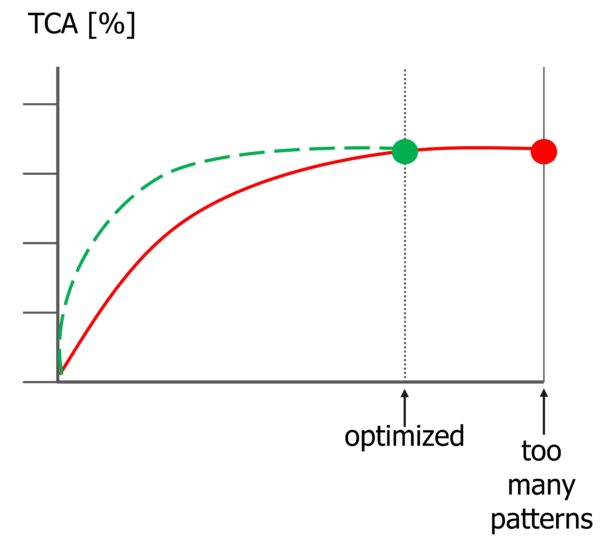
Pattern selection and ordering based on TCA provides a faster coverage ramp, based on the likelihood to detect physical defects compared to traditional approaches, as shown in Figure 1.
Tessent calculates TCA values using physical layout information. A user-defined fault model (UDFM) file stores the models for each defect type (cell-internal, bridge, open, cell-neighborhood). Anyone using cell-aware or automotive-grade ATPG will be familiar with UDFM files. Just load the UDFM files into the ATPG tool to generate test patterns and for use in layout-aware and cell-aware failure diagnosis. When read into the ATPG tool, users can apply the UDFM files containing TCA fault data to patterns to sort them from highest TCA to lowest.
Features of using TCA include:
- Selecting the most effective patterns
- Choosing targets for pattern types and coverage
- Determining the effectiveness of new pattern types
- Grading pattern value by likelihood to detect defects
- Automatically sorting and selecting patterns
- Creating a smaller pattern set by targeting multiple fault models in our ATPG run
High-quality fault models
Underlying the effectiveness of TCA is a toolbox of high-quality fault models, which are also referred to as automotive-grade ATPG. The models include:
Cell-aware: Also called cell-internal, this fault model targets physical defects that can occur within the technology standard cell. The cell library physical design is characterized to produce a user-defined fault model (UDFM) used by ATPG. Cell-aware test models the following types of defects:
- Port open – A disconnected port
- Port bridge – A bridge between a port and VSS, VDD, or any other port of the cell
- Bridge – Any cell-internal bridge defect, such as bridges between adjacent objects in the same layer or different layers. In the case of non-layout-aware runs, bridges are calculated based on parasitic capacitors in the SPICE netlist
- Open – Any cell-internal open defect, such as an open in poly, metal, diffusion, or vias. In the extracted SPICE netlist, the tool matches these defects to existing parasitic resistors by increasing their resistance values
- Ton – Any cell-internal transistor defect that switches a transistor partially on with a specific resistive value
- Toff – Any cell-internal defect that switches a transistor partially off with a specific resistive value
Interconnect: Any bridge or open defect in the interconnect
Inter-cell bridge: Also called cell neighborhood defects, these are chip-dependent bridge defects located at the interface between one instance of a standard cell and a neighboring cell. Such defects can occur between cell-internal nets (layers) not directly accessible from the cell interconnect nets.
Pattern selection, grading and sorting based on critical area
DFT engineers can compare patterns for multiple fault models and select the most effective of each using a consistent and realistic metric. The order_patterns command in Tessent can read in multiple patterns created for various fault models and sort them from the highest TCA to lowest. The only restriction is that fault models for static and dynamic patterns must be sorted separately. Figure 2 shows how to load various fault models to optimize your pattern set. Use these models to simulate and calculate the TCA for an existing pattern set or to create a new pattern set from scratch. Tessent will generate reports show the TCA included during ATPG, summary coverage, fault list, and a layer-based TCA summary.
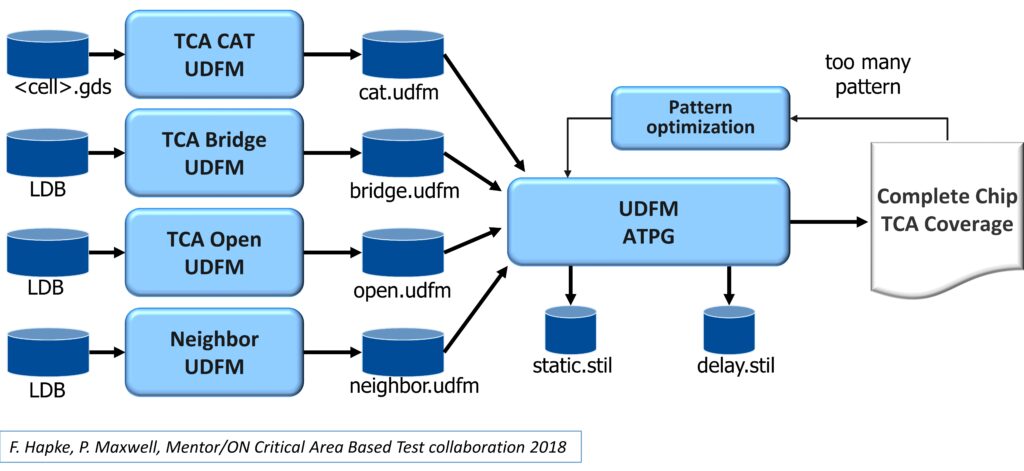
Once you create UDFM files with TCA data for the various fault models, you can grade and sort any existing pattern set based on TCA. This is true even for patterns created without any TCA considerations, such as stuck-at patterns. The steps to sort existing patterns based on TCA are:
1. Load the UDFM files for the various fault models that you want to use.
2. Load the existing pattern sets.
3. Simulate the patterns using TCA from UDFMs.
4. Sort the patterns.
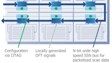
Tessent Streaming Scan Network (SSN)
The Tessent solution for packetized delivery of scan test patterns is proving to be a once in a decade advancement in DFT for complex designs, particularly those demanding high quality. It enables simultaneous testing of any number of cores with few chip-level pins, plus reduces test time and test data volume, figure 3. With SSN, DFT engineers have a true SoC DFT solution without compromises between implementation effort and manufacturing test cost. The inclusion of SSN also vastly reduces the overall DFT architecture complexity so also reduces over all time to market.
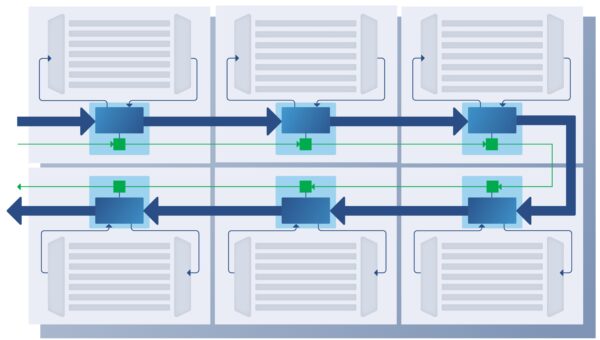
Figure 3. Tessent Streaming Scan Network distributes packetized scan test data to multiple cores across a synchronous bus.
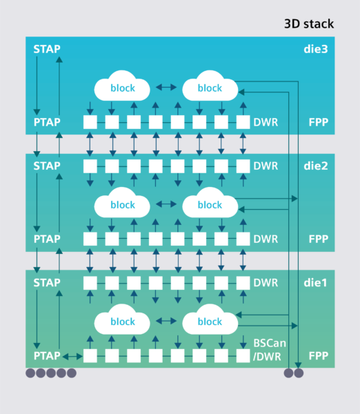
High-quality test for 2.5D and 3D designs
Chiplets integrated on a common interposer (2.5D) or stacked on top of each other (3D) have special considerations for quality that DFT addresses. For 3D IC logic test, we have these high-level considerations:
- Fully testing individual die at wafer level because some die pins are not available for probe by automatic test equipment (ATE).
- Choosing a technology for efficiently performing die-to-die test in the package. The interposer for 2.5D and through-silicon vias (TSV) or micro bumps for 3D stacking are examples of methods for inter-die connection. These die-to-die connections also need to support a repair mechanism to help recover yield loss.
- Choosing how to access any die(s) in the package for sufficient tests.
- Automating failure diagnosis for inter-die and intra-die failures.
Fully testing die at the wafer level is a matter of high test coverage using advanced fault models. Including only known-good die in a stack is a major requirement of successful 2.5D and 3D packages. But it’s not the only requirement.
The Tessent Multi-die software automates test for 2.5D and 3D designs through execution of the IEEE 1838 standard. Tessent Multi-die ensures compliance with the standard, which is crucial to support the multiplex of collective dies stacked into a package (Figure 4).
The role of diagnosis and failure analysis
DFT doesn’t end with detecting manufacturing defects. It also works to improve the manufacturing process and increase yield, which has a direct impact on business. Manufacturing test collects a massive amount of data from failing tests, revealing valuable information about the mechanisms that cause the circuit to fail. Designers and product engineers can analyze this data through scan diagnosis to find the true causes and locations of circuit failures. Scan diagnosis improves the success of physical failure analysis used to validate the defect mechanism.
Fixing a systematic yield problem requires data about the failure mechanisms on an entire population of failing die across wafers and lots. Performing volume scan diagnosis, an advanced technique that uses statistics and machine learning, speeds yield ramp for new processes and improves yield for mature processes. This technology is in use in many successful companies.
Tessent offers industry-leading software for volume scan diagnosis that leads to improved IC quality, including a solution with industry partner PDF Solutions to improve yield ramp and solve yield limiters through volume manufacturing (figure 5).
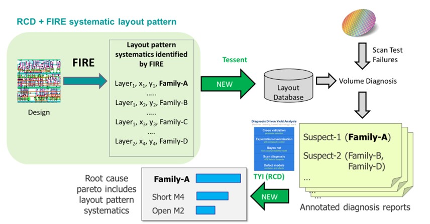
Figure 5. Layout pattern, diagnosis and root-case deconvolution (RCD) flow with Tessent and PDF Solutions.
Summary
Achieving target quality metrics in today’s chips requires careful planning throughout the design process. DFT is critically important for manufacturing high-quality silicon and Tessent offers industry-leading solutions that help designers efficiently meet their quality goals.
Tessent Safety and Security solutions from Siemens EDA offers a range of software and IP to ensure the highest quality ICs.