Three ways to slash AI chip TTM with advanced DFT and silicon bring-up

Advanced EDA technology eases AI chip development
The demand for powerful AI accelerators is growing quickly as new AI models like Chat GPT proliferate. Meeting this demand has pressed AI chip makers with aggressive time-to-market goals, leading design teams to improve their chip development from initial planning to shipping the final packaged IC.
Each stage of design is a candidate for improvement, including design-for-test and silicon bring-up, which can have significant impacts on both the quality and the time-to-market of AI chips. Finding the right tools has a clear return on investment by increasing engineering efficiency, streamlining the development process and getting the product into customers’ hands faster.
AI chips and DFT
The AI chip architecture and test requirements have an impact on the DFT implementation strategy. No matter what the architecture, the AI chips typically have the following design characteristics: Large designs with billions of gates, a large number of replicated processing cores and distributed memories. Designers need EDA tools that address the challenges of each of these AI chip characteristics.
For DFT and silicon bring-up, a tool solution should be able to do these three things to speed up AI chip development time:
- Exploit AI chip regularity
- Shift-left DFT
- Eliminate DFT-to-test iterations
Hierarchical DFT exploits AI chip regularity
AI chips typically contain a large number of identical cores, so all the DFT work—including test insertion, test pattern generation and verification—can be done faster with a hierarchical methodology. All the work is completed just once at the core level, then the complete, signed-off core is replicated automatically to complete the chip-level DFT implementation.
The Tessent TestKompress tool is the industry-leading hierarchical DFT tool. It lets you sign off DFT of blocks at any level of hierarchy, reducing DFT time and effort, test time and test data volume. In the example shown in figure 1, there are three levels of hierarchy: core (tile), block (supertitle), and chip. The core is instantiated multiple times in the block which is then instantiated multiple times at the chip level.
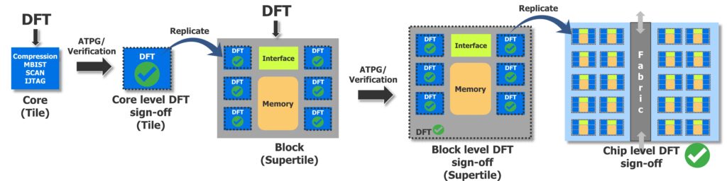
Tessent hierarchical DFT is supercharged by also using the packetized scan data architecture approach provided by Tessent Streaming Scan Network (SSN). With SSN, all the top-level blocks can be connected to an SSN bus that delivers the packetized scan data. Block configuration data is delivered to each block via the IJTAG network. DFT signals are then locally generated from the SSH (Streaming Scan Host) IP, enabling each block to run independently. SSN dramatically reduces DFT implementation effort on large AI chips, which translates directly to faster time-to-market.
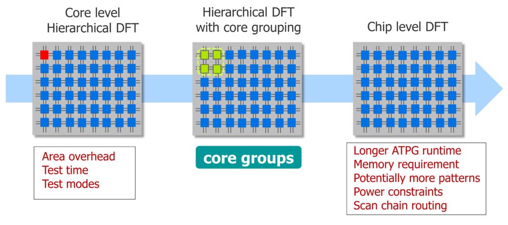
How do you find the most efficient hierarchy in your AI chips to optimize ATPG runtime and area overhead? Performing DFT at the lowest, individual core level incurs some area-usage penalty because the DFT logic like isolation wrappers, compression logic, memory BIST controllers are duplicated in each core. But implementing all DFT at the chip level results in longer ATPG runtime, large memory requirement to load the entire design, layout challenges when routing scan chains through all cores to the compression engine and test power constraints because all scan chains are active at the same time.
The sweet spot for DFT then, is with core groups that balance area overhead with development time overhead, as shown in figure 2. This implementation groups multiple cores together for DFT often referred to as a super core or tile. All the DFT logic is inserted and signed-off at the core group level and SSN can better manage and balance the test pattern delivery.
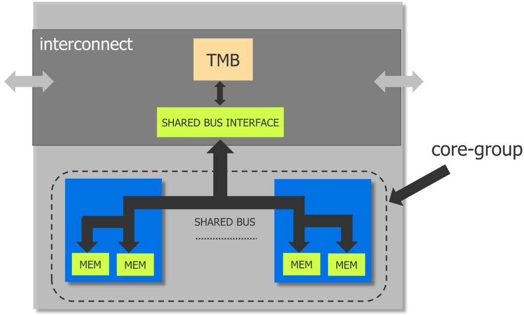
You can also reduce the area overhead of memory BIST controllers when developing AI chips by sharing a memory BIST controller between multiple memories in multiple cores with Tessent MemoryBIST. A shared-bus implementation lets you optimize the memory access bus for routing and timing and to provide the memory BIST controller connection interface (figure 3).
To learn more about shared bus memory testing, read the technical paper Automation of shared bus memory test with Tessent MemoryBIST.
Hierarchical DFT and Multi-die architectures
AI chips using multi-die 2.5D, 3D and 5.5D packaging can use the same hierarchical methodology and the IEEE 1838 standard along with the Tessent Multi-die tool to implement the standard, including the flexible parallel port (FPP). Tessent SSN is well suited to act as the FPP, which further eases the implementation. When using SSN at the die level, moving to multi-die is just an extension of the architecture rather than a completely new architecture.
Hierarchical failure diagnosis
AI chips can also use hierarchical failure diagnosis after the IC is manufactured using Tessent Diagnosis. It allows for core-level diagnosis, which significantly accelerates the process of diagnosis and failure analysis. This hierarchical diagnosis methodology aligns perfectly with the AI chip architectures, which contain repeated identical processing cores.
Shift left – insert DFT at RTL
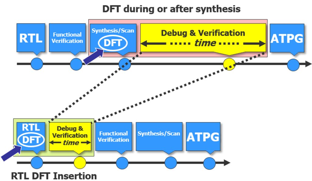
DFT logic is traditionally inserted at the gate-level design during or after synthesis, which suffers from two significant drawbacks.
- The gate-level design is usually larger than the RTL, so it takes much longer to simulate and debug. RTL compile and regression debug runtime can be up to 4 times and 20 times faster than gate compile and regression debug runtime respectively.
- Any changes in the DFT logic or configuration requires another synthesis iteration of the entire design before verification can be performed.
For a huge AI chip, repeating simulation, debug, and synthesis for each iteration adds significant delay to the design schedule. If you insert DFT logic in RTL with Tessent RTL Pro, the delays are minimized because any DFT changes can be verified and debugged faster in RTL without the need of going through the synthesis step. Also, RTL DFT insertion also allows for early I/O and floor planning of the chip. This process significantly shortens the design development cycle. The difference between DFT during or after synthesis and DFT at RTL is illustrated in figure 4.
Tessent RTL Pro also performs testability checks and fixes. Designers can achieve higher test quality in less time by performing all the DFT checking and fixing most testability issues at RTL before running ATPG.
Eliminate DFT-to-test iterations – connect DFT with ATE
Reducing the time spent on silicon bring-up is critical in getting AI chips into the hands of customers. Traditional silicon bring-up typically involves multiple iterations between the DFT domain and the test/ATE domain for pattern debug, characterization, test optimization and test scheduling. There is often a back-and-forth interaction between DFT engineer with test logic knowledge and the test engineer familiar with the tester, illustrated in figure 5.
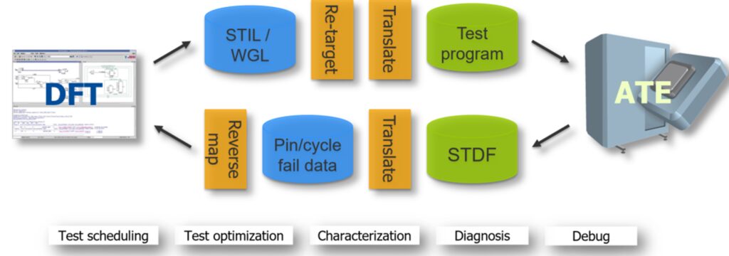
This flow can be vastly improved with Tessent SiliconInsight, which lets DFT engineers perform the silicon bring-up themselves. The test engineers can then run diagnosis in several resolutions from flop- level to net-level without the help of DFT engineers. This solution speeds up the entire process by eliminating the time-consuming and costly iterations between DFT and ATE domains.
Conclusion – Advanced DFT and silicon bring-up solutions accelerate AI chip development
The Tessent software from Siemens EDA is well suited to addressing all of the challenges faced when designing AI chips including. The key tools include:
- Tessent TestKompress – for core level ATPG pattern generation
- Tessent SSN – for optimized packetized scan-based pattern delivery ideally suited for applications with many identical cores
- Tessent RTL Pro – for RTL-based hierarchical DFT construction
- Tessent Multi-die – for DFT of multi die devices
- Tessent SiliconInsight – for reducing iterations in silicon bring-up
Learn more
Read our new technical paper about using advanced DFT and silicon bring-up to accelerate AI chip design.