How to master DFT for tile-based designs

Tile-based IC design flows are predominant in today’s chips. A tiling style affects design-for-test (DFT) and calls for special attention to handling how scan channels are distributed across tiles. Tessent products can support tile-based designs from boundary scan, IJTAG and memory BISR chain routing, Streaming Scan Network, and scan retargeting. DFT for tile-based designs was a hot topic at Siemens User2User meeting this year, and now the video of Vidya Neerkundar describing it is available to view on demand.
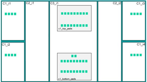
Take this example tiled design with 3 unique tiles. C1 and C2 are mirrored on either side of C3. The physical blocks are abutted and there is no logic at the chip level.
The DFT approach to a tiled design like this would be:
- Use hierarchical design flow
- Top-level floor planning
- Streaming Scan Network (SSN) for logic testing
- Clocking: insert on-chip clock controller (OCC) in each tile
- IJTAG, memory BIST, built-in self-repair (BISR) for tile-based designs
- Embedded boundary scan and Boundary Scan Description Language (BSDL) extraction at chip-level
So how do you access the logic inside the tiles for testing? There are some challenges. Tiles will need varying numbers of input and output channels for compression, how do you allocate and route the chip IO pins to these channels? Can you efficiently broadcast data to identical tiles? How do you balance pipeline stages from chip IO pins to the channels?
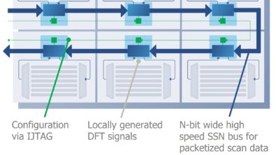
Tessent Streaming Scan Network (SSN) is key to DFT for tile-based designs
A fundamental requirement in testing tile-based designs is the need for test compression with an access mechanism like a bus to transfer packetized test data, which is what Tessent Streaming Scan Network (SNN) does.
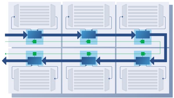
SSN was designed to distribute scan data across abutted tiles. The uniform bus travels the chip in a plug and play manner—there is no need to plan requirements for each tile up front. Using SSN can cut DFT development time in half. It lets designers decouple the core and chip level DFT and define the core grouping at retargeting time. Routing and timing closure is easier because it eliminates top-level muxing. SSN also reduces test time and test volume by up to 4X because:
- Packets are 100% scan data payload
- There is less need for padding in test data
- Core compression is optimal
- Time multiplexing
- Identical cores are tested at constant cost, with diagnosis support
The flexible, adaptable, and silicon-proven SSN is quickly becoming a fundamental solution for the DFT demands of today and tomorrow.
Watch the video for details on the DFT flow for tile-based designs, including clocking, inserting IJTAG, memory BIST and BISR, inserting boundary scan and BSDL extraction, creating DFT ports on tiles and connections between tiles, and simulation views of tiles.