Webinar: Smarter DFT architecture for advanced SoCs
Leonardo DaVinci said that “Simplicity is the ultimate sophistication.” Semiconductor design is a very complex process, and every step of that process introduces risk. Every company wants to reduce that risk and get from concept to hardware as predictably as possible without unexpected delays and costs. Automation is the tried-and-true method, but not all automation keeps up with the ever-increasing complexity of semiconductor design.
The purpose of electronic design automation (EDA) software is to solve SoC design problems and simplify the entire process. For design for test (DFT), this means aiming to streamline the DFT development for today’s large and complex designs. The technologies and methods developed through partnerships between EDA suppliers, foundries, and semiconductor companies should effectively reduce risk, improve time-to-market, and provide a more predictable and reliable DFT solution.
Siemens DFT experts are offering a webinar on 01 March, 2022 that will describe:
- New approaches to SoC test that address scaling challenges
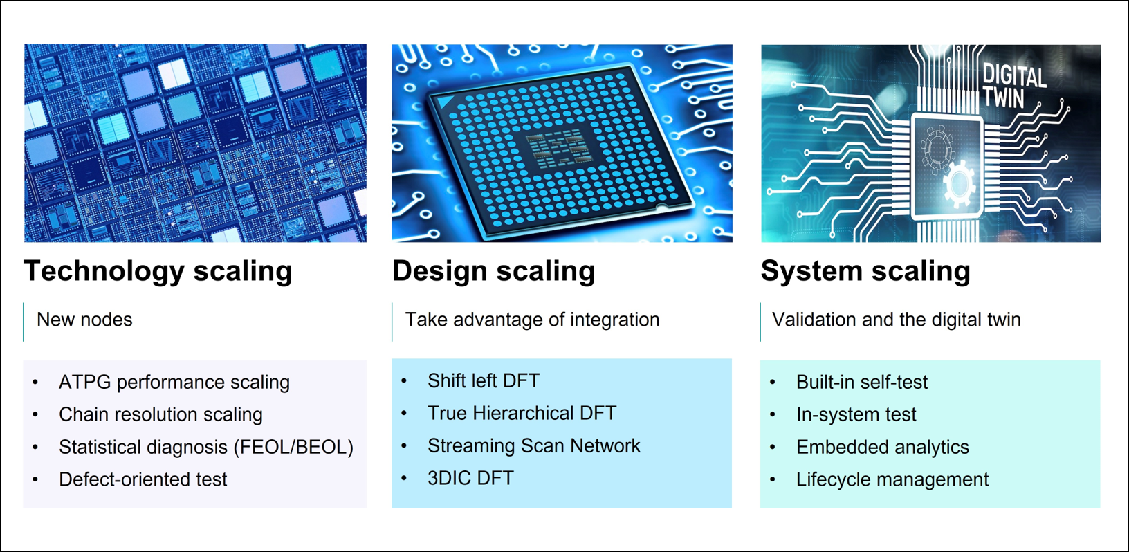
- Hierarchical DFT, packetized scan data, and design architecture
- How to use new solutions for easier DFT development, test, diagnosis, and lifecycle management
Register for this free webinar
Success with automation
When you have a large, complex problem, the solution could be to introduce more automation, more steps, more iterations and maybe add some artificial intelligence algorithms to process complex analyses and tradeoffs.
But sometimes the better solution is to remove complexity. Hierarchical DFT does this. A plug-and-play solution makes core-level DFT independent from the SoC-level embedding. Packetized test data makes the core-level test independent from the top-level IOs. Both of these technologies greatly simplify the problem, removing iteration and optimization steps entirely. Failure diagnosis, likewise, works with the hierarchical layout to simplify the process of identifying and locating faults.
Design teams need to think of DFT from the SoC level and ensure the DFT architecture is good. There are a few newer technologies that streamline and simplify any DFT project—IJTAG, Streaming Scan Network (packetized scan delivery), on-chip compare in cores, and hierarchical DFT. Many of these solutions are embedded in existing EDA software and others are new, but each has demonstrated significant advantages in real designs.
Register here to learn about approaches for SoC DFT that simplify the problems introduced by technology, design, and system scaling. These methods have been shown to significantly reduce risk, improve time-to-market, and provide a more predictable and reliable DFT solution.