For secure chips, use high-quality test and embedded analytics

There is growing concern over the security of ICs used not just in aerospace and military devices, but also in smart cards, medical, automotive, and datacenters. A broad range of chips now need to ensure that sensitive data is inaccessible to outside agents, making the requirements around secure test and monitoring mainstream. The current best strategy is to add security across different levels of SoC development to provide the best coverage in a defense-in-depth solution.
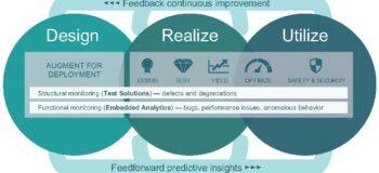
Figure 1 above illustrates a high-level concept of device security across the ecosystem.
At the level of System Integrity (from figure 1), chip makers need to be concerned that the normal test structures on the SoCs can compromise any functional security features already part of the design.
So, what are some security risks of common IC test strategies? How can we mitigate them?
Scan-based test vulnerabilities
Scan chains provide full access to the sequential elements of a device under test. Serial access from device pins allows test patterns to provide the stimulus and response needed to detect defects. Historically, scan test achieves the highest achievable test quality with low design and schedule impact.
However, while fully accessible scan chains are great for test, they are vulnerable to scan-based side-channel attacks. Many designers of secure applications have been seeking alternate approaches that provide the benefits of deterministic scan test while maintaining the required IC security.
Test access mechanism can be vulnerable
In addition to scan chains, most designs now have some form of test access mechanism (TAM), such as an external interface IEEE 1149.1 (JTAG), or both an external and internal interface with an in-system test controller which is used for running in-system test.
The test access port (TAP) is mostly used for setup, configuration, running and data collection of various complex test structures within the design. The TAP gives direct access to many critical registers within the design. Access to these registers could be used to collect sensitive data or, in some cases, program the device to operate outside its intended function. To keep the TAP from acting as a simple back door to the design, it must be as secure as the other functional interfaces within the design.
There are several ways for designers to mitigate the security risks associated with common test structures:
- Apply functional test patterns—these patterns can be created by the chip design team in a closed environment and applied in a secure tester environment, but these can be very time consuming to create and inefficient in terms of their coverage of the logic.
- Use logic BIST—pattern generation, application, and responses are all fully contained on the chip, this removes any direct access to scan chains
- Use embedded test compression—compressed scan inputs and outputs help protect against scan-based side-channel attacks
- Adopt a bus-based packetized scan data distribution—adds more security to embedded test compression because access to the scan chains has an additional level of abstraction
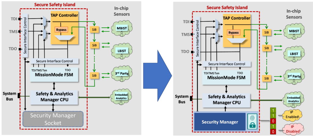
- Secure the test access mechanism—make an embedded safety island to allow for secure in-life analytics data collection (figure 2)

Figure 2 – Security manager socket architecture
Security risks to ICs can be mitigated with strategies applied across the design and manufacturing environment to build multiple rings of defense. This defense-in-depth strategy would include using existing test technology to introduce many levels of protection against malicious attacks. Although some of these concepts are passive – they just providing a lock against access – others are also reactive in that they can take evasive action when a threat is detected.
Learn more in the technical paper available here:
https://resources.sw.siemens.com/en-US/white-paper-high-quality-test-and-embedded-analytics-for-secure-applications


