Improve defect detection for competitive, high-quality SoCs
To deliver the highest quality SoCs, these manufacturing test strategies ensure defects are detected before it’s too late.
It is more important than ever for semiconductor companies to guarantee very high-quality devices. The path to near zero-defect SoCs involves boosting defect detection through the use of test technologies that provide automotive-grade quality of test.
Siemens has industry-leading design-for-test software that helps semiconductor companies stay competitive. Here are two leading technologies with resources so you can learn more.
Critical area-based test
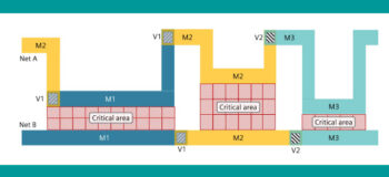
Critical area-based pattern optimization can help define which test patterns are the most important. The use of total critical area (TCA) to choose the types of patterns to apply takes the guesswork out of picking the most effective patterns. With new critical area automation, the tool determines the likelihood of defects occurring based on their critical area. This enables you to sort the various pattern sets not just by the detected faults, but by the likelihood of defects for those faults to choose the most effective patterns to apply.
TCA provides a common metric to assess a pattern’s impact on defects detection, which can be used to sort or order patterns to achieve the lowest defects per million (DPM). As a result, you can mix in patterns targeting new fault models for a more effective pattern set, even with the same number of patterns as your original pattern set. You can select or sort the most effective patterns from your entire pattern set based on their ability to detect physical defects.
Why is critical area-based pattern optimization a game-changer for test? Because test coverage targets for static and dynamic patterns targeting stuck-at and transition fault models, respectively, are usually based on the percent of faults detected. These targets vary by company and it often takes years of production fail data to decide on appropriate goals. When a company needs to add a new fault model, the target could be completely different from test coverage based on the full fault list. For example, consider targeting a test coverage for all potential bridge faults—this could be a huge list. You might achieve 99% detection of all bridge faults but still miss hundreds of the most likely bridges. To reduce DPM, it is more effective to choose the subset of bridges that is most likely to occur.
With the critical area-based pattern optimization in Tessent, you can :
- Select the most effective patterns
- Choose targets for pattern types and coverage
- Determine the effectiveness of new pattern types
- Grade pattern value by likelihood of defects occurring
- Automatically sort and select patterns
- Create a pattern set up to 40% smaller by targeting multiple fault models in one automatic test pattern generation (ATPG) run
Learn how critical area-based test works and how it can improve the quality of your ICs by watching this on-demand webinar
Using critical-area weighted optimization for more effective test patterns.
Small delay, Cell-aware test
Among the pattern types that will find more defects are the cell-aware patterns that target defects within cells for significant reductions in defective part levels. Cell-aware test targets specific shorts, opens, and transistor defects because it characterizes each cell through analog simulations. Cell-aware ATPG is just part of the larger class of defect-oriented test, which uses physical design data to ensure that defects aren’t missed and provide automotive-grade quality of test. Intel used the Tessent cell-aware, defect-oriented test to reap stunning reductions in DDPM.
Hear about Intel’s experience with Cell-Aware test from Will Howell, Intel Principal Engineer, in this video
Intel dramatically improves test quality with Tessent Cell-Aware test.
Small delay defects are also important for many types of devices to detect marginal defects that only manifest themselves on paths with small slack margins. While traditional transition at-speed scan testing does not target small delay defects, timing-aware ATPG automatically finds these small slack margins in the design and targets them. Timing-aware ATPG has been shown to be an effective way to generate high-quality test sets that detect small delay defects through the longest paths. Cell-aware test can also focus ATPG on the largest delays within the cell. Combining timing-aware ATPG with small delay cell-aware test provides significant unique detection of defects.
Learn about timing-aware ATPG and the benefits of combining timing-aware ATPG with small delay cell-aware test in this video
Timing-Aware ATPG – Small Delay Defect Detection.
Leveraging critical area-based pattern optimization and Cell-Aware test with small delay defect detection can limit defective products from being shipped, which is business-critical in the competitive market for mission-critical ICs.