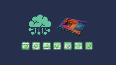
Discover how Siemens’ EDA evolution of machine learning in the physical design and verification of semiconductor packages.
Explore this infographic to learn why a comprehensive workflow essential for chiplet design and today’s 3D IC architectures.
Scalability and range of IC packaging design solutions In my last blog, I talked about multi-domain and cross-domain integration that…
Multi-domain integration enables faster time to market for complex advanced semiconductor packages with a seamless integration of design and verification.
If you’re involved in semiconductor package design using routable substrates — that is, as opposed to leadframe based — then…