Getting your metal fill right
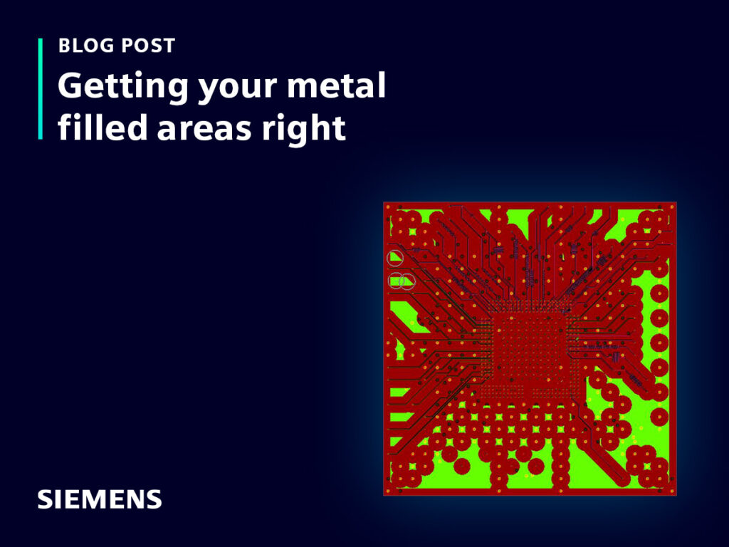
If you’re involved in semiconductor package design using routable substrates — that is, as opposed to leadframe based — then you will most likely be creating metal filled areas. Metal fill is typically used for planes as well as signal shielding, but it can also be used for the benefit of manufacturing to help prevent substrate warpage.
Problems with large areas of metal fill in manufacturing
When you create large areas of metal, you can also create manufacturing issues. The first and most obvious is around the actual successful creation that meets the manufacturer’s often stringent criteria. Then there is substrate warpage, where uneven conductor densities on the same layer or across layer pairs can cause warpage and another around outgassing or offgassing. During the substrate build-up and RDL manufacturing process the dielectric and metal layers can suffer from areas of delamination due to trapped pockets of gas caused by materials using in substrate manufacturing containing salts or organics that create the gas during the fabrication process.
This obviously impacts the production yield of the substrate, as well as the reliability and lifecycle of the device. Think of it being like adding a screen protector to your smartphone and how hard it is to get the air bubbles out. So as a result, substrate fabricators and manufacturers do not like solid metal planes or large metal areas. To avoid such issues, they typically provide designers with strict metal fill requirements in the form of rules, design rule checks, and often a design rule manual (DRM).
As you can imagine the combination of these issues and all the rules makes the designer’s job of meeting the fabricators acceptance criteria a challenge. Further, the diversity of substrate technologies from numerous vendors means there’s no one-size-fits-all solution.
Methods to control metal fill issues
However, there are three methodologies that are typically used by designers to mitigate/control issues. The first is hatched filled metal areas with layer offsets. The second is the insertion of outgassing void patterns and the third is the addition/insertion of dummy metal fill.
These are the most common methods to achieve the substrate fabricators requirements for metal areas and planes in advanced package designs such as interposers, high-density-fan-out wafer level package (HDFOWLP), and high pin count flip chip BGAs, so it is important to understand how to use them efficiently and effectively in order to prevent extended design cycles or ECO’s due to fabricator rejection of the design.
An applications expert within Siemens Technical Solutions Sales has authored a very descriptive technical paper on this topic. To learn more about how to use these three methodologies successfully, download the paper, “A Proven Methodology to Meet Manufacturing Process Requirements for Metal Filled Areas and Planes.”