Unlock advanced chiplet design success: Discover the Siemens EDA Heterogeneous Integration eBook series
The future of semiconductor innovation is rapidly shifting from monolithic chips to advanced, multi-chiplet architectures. As devices demand greater power, smaller footprints, and increased functionality, integrating multiple chiplets—each with specialized abilities—has become the cornerstone of competitive hardware design. But tapping into the promise of chiplet integration demands a new design methodology.
For engineers and system architects, this means navigating new terrain—with new complexities, challenges, and opportunities. Fragmented workflows, ad-hoc connectivity, and siloed verification can lead to costly respins, delayed schedules, and performance shortfalls. That’s why Siemens EDA has put together a comprehensive eBook series designed to walk you through a proven methodology for successful heterogeneous integration, covering everything from those crucial initial planning stages all the way to final sign-off.
This series isn’t just about theory; it offers a practical, system-wide approach to help you master multi-chiplet designs. It’s all about optimizing power, performance, area (PPA), cost, and reliability across your entire system – from the silicon itself to the package, interposer, and PCB.
If you’re attempting advanced packaging, this series will provide you with the strategies and insights you need to overcome common design hurdles, simplify your processes, and achieve superior results in an increasingly interconnected design environment.
What’s inside the Heterogeneous Integration eBook series?
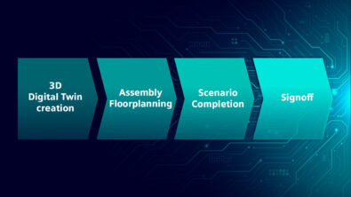
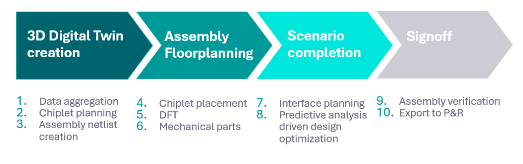
The series covers a 10-step methodology formulated by Keith Felton, IC Packaging product marketing manager at Siemens EDA.
Each eBook delivers expert guidance and practical methods to help you take control of every stage of the chiplet integration journey. Here’s what you’ll find:
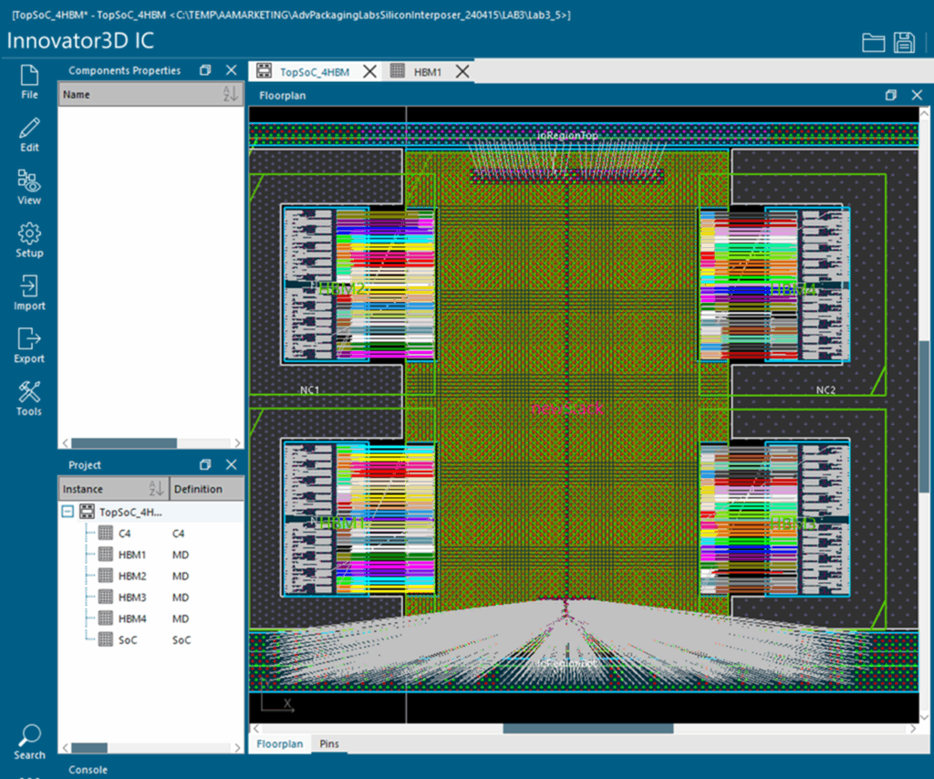
eBook 1: Building your digital foundation
Focus: Constructing a full-system digital twin for advanced packaging projects.
What you’ll learn:
- How to aggregate and standardize diverse design data, overcoming manual bottlenecks.
- Ways to accelerate package design using hierarchical device planning and parameterized building blocks.
- The importance of language-based netlists over error-prone spreadsheets for tracking massive die-to-die connections.
- Formal verification techniques to assure system-wide connectivity and function.
- Why industry standards (like 3Dblox and OCP Chiplet Design Exchange) are vital to future-proof workflows and foster collaboration.
What will you gain from this eBook?
This eBook sets the bedrock for your chiplet projects—a digital twin that drives connectivity, updates, and verification as your design evolves. By mastering data management from the start, you’ll avoid downstream problems and save time.
eBook 2: System technology co-optimization (STCO)
Focus: STCO methodology for optimizing advanced package designs.
What you’ll learn:
- The transition from traditional device technology co-optimization (DTCO) to holistic STCO.
- Chiplet planning, placement, and assembly netlist creation techniques for modern designs.
- How to integrate design-for-test (DFT) and mechanical co-design into chiplet assembly.
- Multiphysics predictive analysis to anticipate challenges and tune designs before fabrication.
- Continuous verification strategies for streamlining workflows and minimizing design iterations.
What will you gain from this eBook?
eBook 2 is your blueprint for system-wide success. By following its STCO roadmap, you can break free from legacy silos and optimize power, performance, area, cost, and reliability across your entire stack.
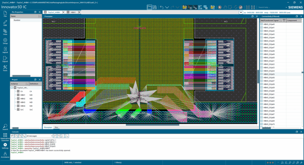
eBook 3: Interconnect planning & electrical optimization
Focus: Chiplet interface data path planning and early multiphysics predictive analysis.
What you’ll learn:
- How to identify and route critical interconnect groups from the chiplet bump field to BGA balls or target locations.
- Steps to maximize signal integrity and electrical performance with minimal routing congestion.
- Early multiphysics analysis methods for assessing chip-package interactions (CPI).
- Planning workflows that account for real estate limitations, noise, crosstalk, and manufacturing constraints.
- Tools and tactics for optimizing the chiplet assembly before detailed implementation kicks off.
What will you gain from this eBook?
Get ahead of costly surprises by perfecting your interconnect plans and validating electrical pathways early. eBook 3 shows how strategic analysis enables first-pass design success and boosts time-to-market.
eBook 4: Mastering sign-off
Focus: Verifying and signing off heterogeneous integrated designs, including physical verification.
What you’ll learn:
- The unique challenges of package-level verification and why IC-centric solutions aren’t enough.
- How assembly design kits (ADKs) and standardized rules streamline physical verification.
- Steps for layout-versus-schematic checks, data export and handoff, and team coordination.
- Strategies to collaborate across multiple substrates, processes, and manufacturing vendors.
- How Siemens’ automated tools and rule-driven workflows deliver reliable signoff and minimize risks.
What will you gain from this eBook?
Don’t let verification bottlenecks derail your launch. This eBook equips you with a comprehensive approach for closing the design loop, ensuring manufacturability, and scaling with confidence—even as complexity grows.
Transform your 3D IC projects from concept to signoff
If you’re looking to accelerate new product introduction, reduce costly respins, and stay competitive in an evolving landscape, this eBook series provides both vision and tactical guidance. Each volume delivers expert-backed methodologies, practical workflows, and actionable tips tailored for system architects, design engineers, and verification leaders.
Whether you’re mapping out your first chiplet architecture or seeking to streamline complex package verification, these eBooks offer an invaluable resource for ongoing success.
Download them all today!