Scaling 3D IC design: Trends, challenges and practical workflows, Part 2
Managing strategic risk, cost of ownership and time-to-market in the AI era
Authors: Kevin Rinebold and Andras Vass-Varnai, Ph.D.
In this second blog in a two-part series our expert team distills critical insights from a recent Siemens webinar featuring Kevin Rinebold and Andras Vass-Varnai, Ph.D. from Siemens, alongside Brendan Burke, Research Director, Futurum Group, with datapoints provided by Futurum Research.
Together, they examine the evolving semiconductor design landscape shaped by the shift from the era of monolithic dies to the new era of heterogeneous architecture, offering a blueprint for navigating the complexities of AI-driven 3D IC and chiplet technologies. This transition is redefining the strategic management of costs, risks, and time-to-market, empowering teams to address the challenges of next-generation semiconductor innovation.
From monolithic scaling to heterogeneous integration: New design choices, new business stakes
As the semiconductor industry shifts toward advanced packaged systems, chiplet and 3D IC architectures are becoming essential to meeting rising demands for compute power, efficiency and adaptability in the AI era. In heterogeneous designs, early architectural decisions have an outsized impact on downstream performance, manufacturability and total cost of ownership (TCO). Late-stage changes are no longer just engineering setbacks; they are business risks that can delay product launches and weaken market position.
Why 3D IC success now depends on managing risk, cost and performance early
Digital twin authoring and predictive multiphysics analysis help teams make better-informed decisions earlier in the design cycle, reduce costly rework and improve delivery predictability. This blog shows how semiconductor leaders can use a more connected, system-level approach to balance performance goals with business realities and bring next-generation products to market more successfully.
Executive summary / Key takeaways at a glance:
- The shift: As traditional scaling limitations become evident, the semiconductor industry is actively transitioning toward heterogeneous integration architectures like chiplet-based designs, which are essential in meeting modern AI demands.
- Strategic solution: Implementing System Technology Co-Optimization (STCO) through early multiphysics analysis, strengthened by AI-assisted exploration of design trade-offs, is crucial for addressing complex challenges – including thermal management and integration efficiency – while simultaneously reducing risks and costs.
- Economic implications: The Siemens Innovator3D IC and Calibre 3D IC products, enhanced with AI design space exploration tools, empower teams to manage complexity effectively, leading to faster time-to-market and lower total cost of ownership.
- Operational excellence: The success of this transition relies on adopting a collaborative design culture that values cross-disciplinary cohesion throughout the design and manufacturing processes, ultimately translating engineering excellence into effective production and business outcomes.
- Compelling AI design insights: Andras Vass-Varnai, Ph.D. observes,“We are moving toward AI-based intelligence to simplify and automate the creation of multiphysics flows… providing insights that exceed human experience alone.”
- A practical path forward: Walk through an integrated workflow using Siemens Innovator3D IC to turn 3D IC potential into a scalable reality.
What role does the Digital Twin play as an orchestrator?
As we move into the world of 3D IC, the sheer volume of data, the variety of formats and the number of stakeholders involved make manual design management ineffective.
We have reached a critical inflection point. The complexity of 3D IC necessitates a shift from traditional, single-node thinking to a system-centric approach. This new paradigm is built on four key pillars:
- System-level floor planning: We are moving beyond optimizing a single device. Success now requires managing power, performance, area (PPA) and cost across multiple processes and domains. This requires a full-system perspective that stays consistent from early planning through manufacturing handoff.
- Multiphysics modeling: Performance is no longer just an electrical conversation. Increased effective power density and reduced thermal paths in stacked architectures have made thermal management significantly more challenging. We must also factor in the mechanical reality of 3D structures, such as TIM (thermal interface material) layers, the package lid and even heatsinks along with more traditional package structures such as bumps, through-silicon vias (TSVs) and redistribution layers (RDLs), and how they contribute to thermals, stress and warpage.
- Scalability and continuous validation: We can no longer afford to wait until the end of the cycle to validate a design. We need predictive modeling during the initial floor-planning phase and continuous performance validation as the design matures.
- Multi-die sign-off: Verification must evolve. We need comprehensive design rule checking (DRC) and layout versus schematic (LVS) steps that look at the entire 3D stack as a single entity, rather than just checking individual substrates in isolation.
Heterogeneous system floorplanning
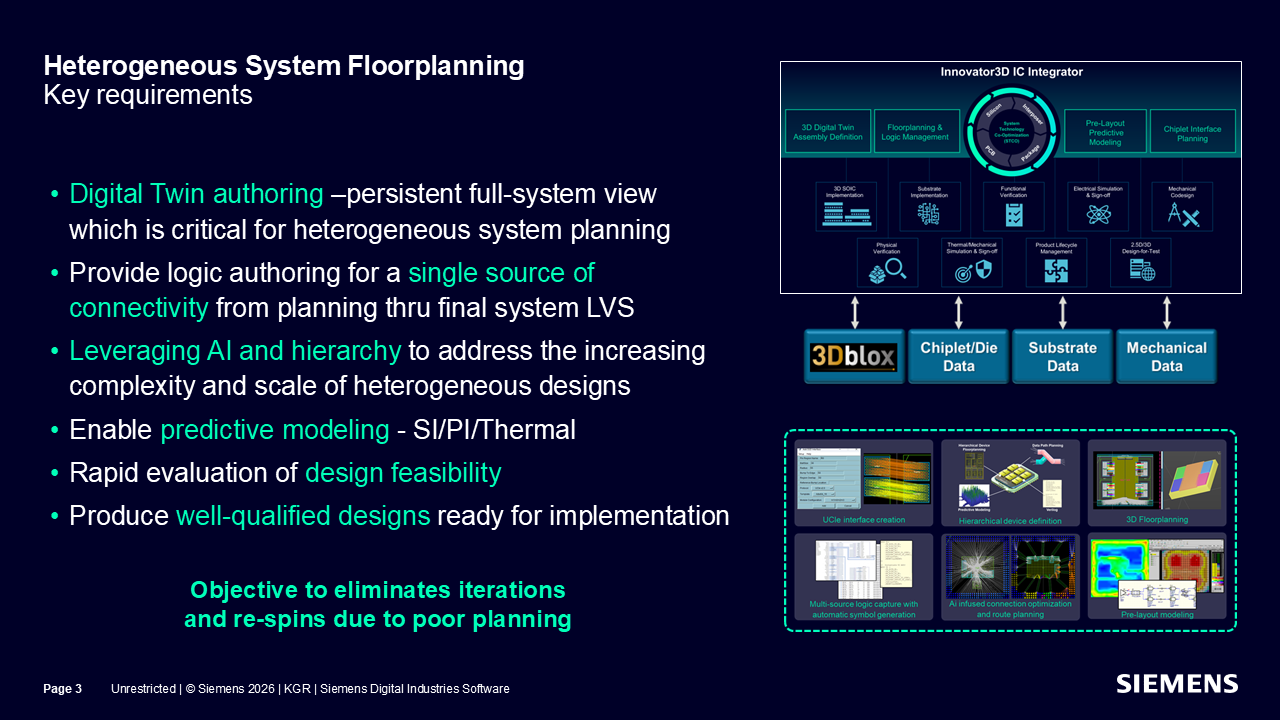
To build a successful 3D IC, you must move beyond fragmented data. We need a mechanism to compile the full system view, what we call the Digital Twin, by aggregating data from different sources, formats and levels of abstraction into a single source of truth.”
–Kevin Rinebold, Technology Manager for 3D IC Solutions, Siemens
This planning cockpit allows all stakeholders, from IC designers to package engineers, access to the same design data, eliminating the need to “reconstitute” the design every time a new team member joins the project. By maintaining a single source of system connectivity from logic capture through final sign-off, teams can perform predictive modeling for thermal, signal integrity and routing feasibility early in the process. The objective is clear: identify and fix issues when they are easier and less expensive to solve, ensuring a well-qualified design that is ready for implementation without costly respins.
The data chaos problem
The primary challenge in 3D IC isn’t just the physics, it’s also the data chaos.
A typical 3D IC project involves IC designers, package engineers and thermal/mechanical experts. Each team speaks a different technical language and uses different file formats:
- IC designers work in Verilog and library exchange format/design exchange format (LEF/DEF)
- Package engineers might use GDS or specialized layout tools
- Thermal experts rely on complex standardized or even tool dependent simulation models
Without a central orchestrator, these teams operate in silos. They pass files back and forth, losing critical context in the translation. This is where the productivity gap begins to widen.
How does Innovator3D IC Integrator solve data chaos?
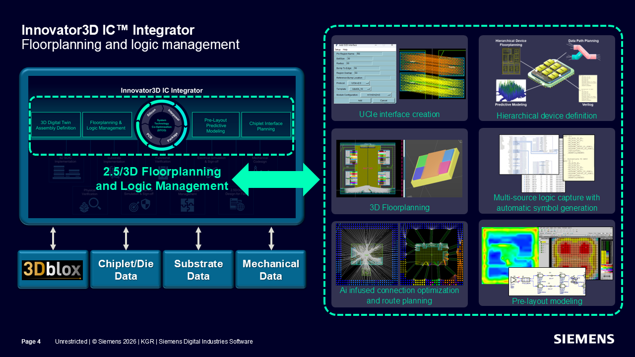
Innovator3D IC Integrator is Siemens’ unified cockpit for planning, floorplanning and predictive multiphysics analysis of 2.5D and 3D heterogeneous systems. It maintains a Digital Twin of the full assembly, from chiplets and interposers to packages and PCB, so teams can work from a single source of truth.
With support for multiple abstraction levels and design stages, it helps teams evaluate power, performance, area and cost trade-offs early, while connecting planning, implementation, analysis, signoff and manufacturing handoff in one cohesive workflow.
Kevin Rinebold observes, “As 3D IC designs grow in complexity, designers need more than just raw performance—they need tools that can effectively manage astronomical data sets. Innovator3D IC Integrator is Siemens’ solution for bridging this gap. It serves as a unified environment for system-level floor planning and multiphysics modeling, providing a persistent Digital Twin that spans the entire design domain.”
The Digital Twin: A single source of truth
Siemens’ approach centers on the Digital Twin. This isn’t just a 3D model; it is a virtual, data-rich representation of the entire system. It acts as the single source of truth that aggregates every piece of data from every team.
By using the Digital Twin as an orchestrator, teams can perform:
- Heterogeneous planning: You can see exactly how a 3nm logic die interacts with a 7nm I/O die and an HBM stack in real-time within the complete context of the system. This approach enables planning and optimization across the entire heterogeneous assembly, rather than just isolated components.
- Predictive analysis: Rather than waiting for a physical prototype, teams can identify thermal hotspots, mechanical stress risks, and other multiphysics issues much earlier in the design cycle.
The human bridge: Speaking the same language
Perhaps the most important role of the Digital Twin isn’t technical, it’s human.
In a traditional workflow, the thermal engineer and the IC designer often only talk when something goes wrong. The Digital Twin changes that. It provides a common visual and data-driven language that allows them to collaborate from day one. It turns a series of hand-offs into a continuous productive conversation.
As Kevin Rinebold notes, “These scalable integrated technologies help teams overcome the widening productivity gap and bring complex 3D IC architectures to market with confidence.”
With a Digital Twin orchestrating your workflow, you aren’t just compressing timelines, you’re securing the operational integrity of the final system.
From AI-powered to AI-driven
Once a Digital Twin exists, the challenge shifts from managing data to exploring the vast number of possible design decisions.
In 3D IC design, pursuing efficient solutions requires evaluating a growing number of architectural, thermal and physical parameters. While human expertise remains vital, manual methods are insufficient to manage this level of complexity.
The shift: From task automation to workflow orchestration
AI capabilities must evolve. While AI-powered tools accelerate discrete tasks, AI-driven workflows enhance coherence by coordinating tools, evaluating scenarios and assisting engineers through intricate design spaces.
This evolution toward agentic AI helps navigate interactions across thermal, electrical and mechanical design domains. The Digital Twin enables AI to help us think bigger, so we can move into the age of agentic AI, where intelligence doesn’t just follow instructions but manages the design space exploration for us.
Andras Vass-Varnai, Ph.D., 3D IC Solution Architect at Siemens, explains:
“The whole point of using agents is that they can pick up these individual tasks, controlling different tools like Innovator3D IC or Calibre 3D Thermal, and manage the design space exploration for you.”
What is design space exploration?
Design space exploration is the use of AI to create, orchestrate and evaluate large numbers of design alternatives across competing objectives and constraints. Instead of relying on manual iteration through a limited set of options, AI can search the design space more broadly and identify candidate solutions that improve metrics such as power, performance, area, thermal behavior and signal integrity concurrently.
In practice, AI-driven design space exploration can assess thousands of what-if scenarios, including placement, floorplanning, routing and packaging trade-offs, to surface options that may not be obvious through conventional workflows or engineering intuition. For example, an AI agent might compare placement alternatives and identify configurations that improve both thermal behavior and signal integrity while preserving implementation targets.
This marks a shift from AI-assisted tools that primarily accelerate tasks to agentic AI systems that can propose, evaluate, and refine design options within defined engineering objectives.
Exceeding human experience
As Andras Vass-Varnai notes: “We are moving toward AI-based intelligence to simplify and automate the creation of multiphysics flows… providing insights that exceed human experience alone.”
This isn’t about replacing the engineer, it’s about augmenting them. By automating the tedious multiphysics flows, AI allows the designer to focus on high-level strategy and innovation.
In the world of 3D IC design solutions, AI is no longer just a tool in the box. It helps engineers evaluate more design options and manage the complexity of advanced 3D IC architectures.
What’s available today — and what’s emerging next
AI in semiconductor design is advancing in stages. Some capabilities are already delivering practical value today in current workflows, while others are emerging as the next phase of design automation. For engineering teams, the distinction matters: today’s AI is helping accelerate analysis, implementation and optimization, while tomorrow’s AI will increasingly connect tools, automate longer-running tasks, and bring far more design knowledge directly into the workflow.
Available today:
- AI-assisted routing, which improves implementation efficiency and helps meet signal-integrity requirements
- Predictive modeling, which evaluates thermal, electrical and reliability behavior earlier in the design process
- Optimization, which automates feasibility sweeps and improves convergence across placement, implementation and verification workflows
Emerging next:
- Autonomous agents, which can take on longer-running design tasks with less manual intervention
- Workflow orchestration, which coordinates complex design processes across multiple tools and engineering domains
- Retrieval-augmented design knowledge, which grounds AI in trusted engineering data, rules and design context to improve decision-making
Together, these emerging capabilities point toward a more connected design environment in which AI can coordinate workflows across tools, surface trusted engineering knowledge at the right time, and support broader design space exploration with greater speed and confidence.
The multiphysics cockpit: Turning data into performance
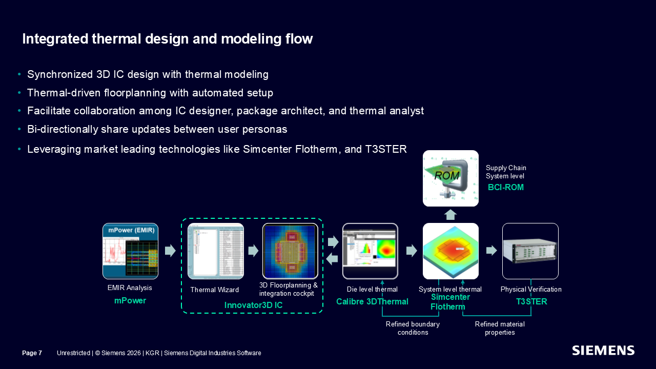
If the Digital Twin is the golden source of truth, then Innovator3D IC is the cockpit where that truth is put to the test. 3D IC design is no longer just about connectivity and netlists; it is about geometry and materials.
To build a stack that survives the real world, we must look at the design through three critical lenses: Thermal and stress, signal integrity (SI) and the collaboration engine.
1. Thermal and stress: Managing the physical reality
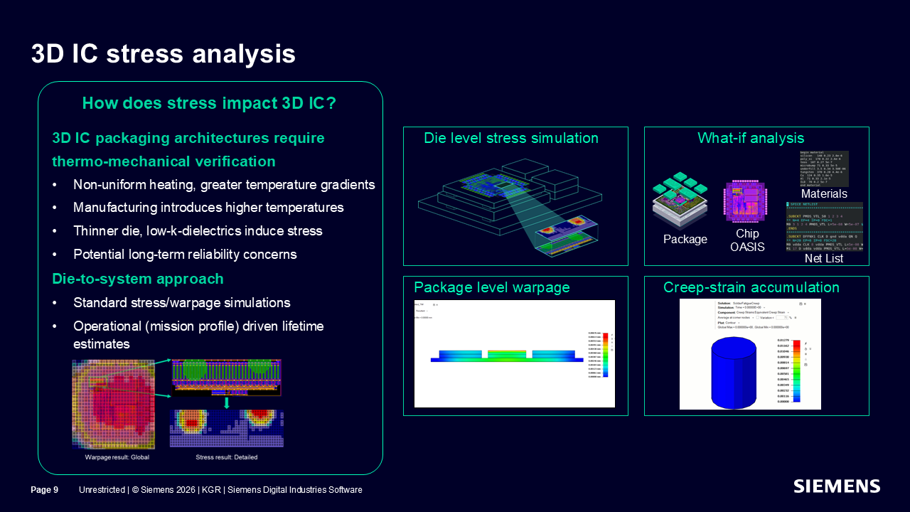
In a 3D stack, heat and mechanical stress are your primary enemies. As Andras observes, “We can’t just guess at these variables; we have to model them with precision.”
- Material matters: The workflow allows designers to assign real-world material properties, following Joint Electron Device Engineering Council(JEDEC) standards, directly to the Digital Twin. Siemens enables you to physically measure manufactured components to verify that material properties are behaving in the real world exactly as predicted by the model.
- Automated precision: For those who aren’t thermal experts, the tool includes wizards that automate complex tasks—like automatically calculating the precise thickness of thermal interface materials (TIM) to fill gaps between dies and packages perfectly.
- Predicting the lifetime: By moving beyond simple heat maps to stress and warpage analysis, designers can predict creep strain in interconnects. This allows you to estimate reliability trends and expected lifetime under defined operating conditions.
2. Signal integrity: The high-speed challenge
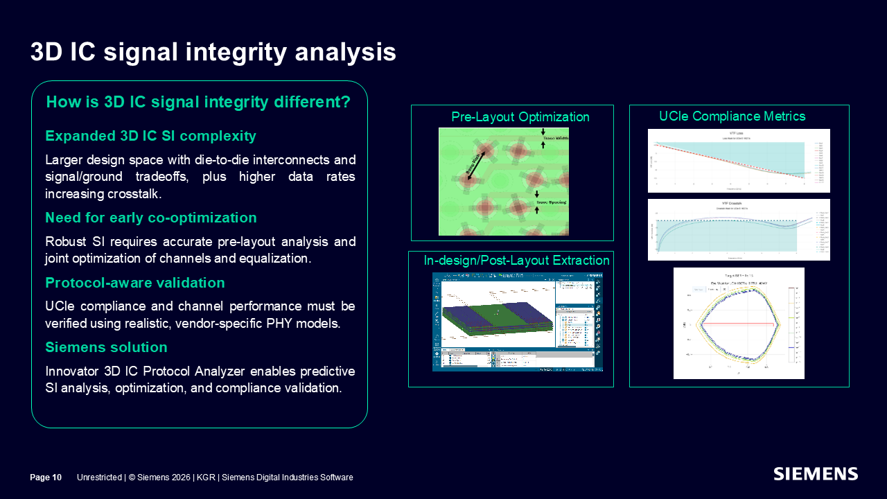
As we stack dies and shrink interconnects, SI problems expand exponentially. High data rates and dense routing create a breeding ground for crosstalk and channel degradation.
- Protocol-aware analysis: The Siemens workflow goes beyond generic analysis to offer protocol-aware validation for interfaces such as universal chiplet interconnect express (uCIE) and other advanced die-to-die interconnect standards. This ensures that your virtual model accurately reflects how the silicon will behave under realistic, vendor-specific conditions.
- Shift-left security and integration: By using predictive, pre-layout analysis, designers can leverage shift-left 3D IC co-design to co-optimize channel structures and equalization techniques before the design is frozen. You don’t even need a finished layout to begin; power data can be pulled in as early as the VHDL description stage, allowing for true architectural exploration.
3. The collaboration engine
Perhaps the most human element of the Siemens workflow is how it bridges the gap between different personas. A 3D IC design solution is a collaborative effort involving:
- IC designers focused on the chiplet
- Package architects focused on the assembly
- Thermal analysts focused on system-level reliability
Innovator3D IC acts as the collaboration cockpit, allowing these experts to work off a single Digital Twin. It enables IP-protected sharing, creating reduced-order models that let you share critical thermal data with board-level teams without disclosing your sensitive floorplan or layout secrets.
The future: Solving the expert’s dilemma with Agentic AI
The move toward AI-based intelligence is very exciting. We are entering a three-stage evolution:
- Goal definition, large language model (LLM): Using natural language to set performance metrics and design intent.
- Agentic AI: Intelligent “agents” that take control of individual tools (like Calibre or Flotherm) to manage the design space exploration for you. These agents leverage skill databases and RAG (Retrieval-Augmented Generation) and can leverage organizational knowledge captured from previous projects.
- Optimization: AI-driven engines that explore thousands of what-if scenarios to find the perfect balance.
The human payoff: Even the most experienced engineer struggles with concurrent contingencies. For example, SI wants components close together to reduce latency, but thermal management wants them far apart to dissipate heat.
Agentic AI can navigate these conflicting requirements simultaneously, providing insights that exceed human experience alone. It doesn’t replace the engineer; it gives them the superpowers needed to master the most complex architectures ever built.
The Path to the next decade of innovation
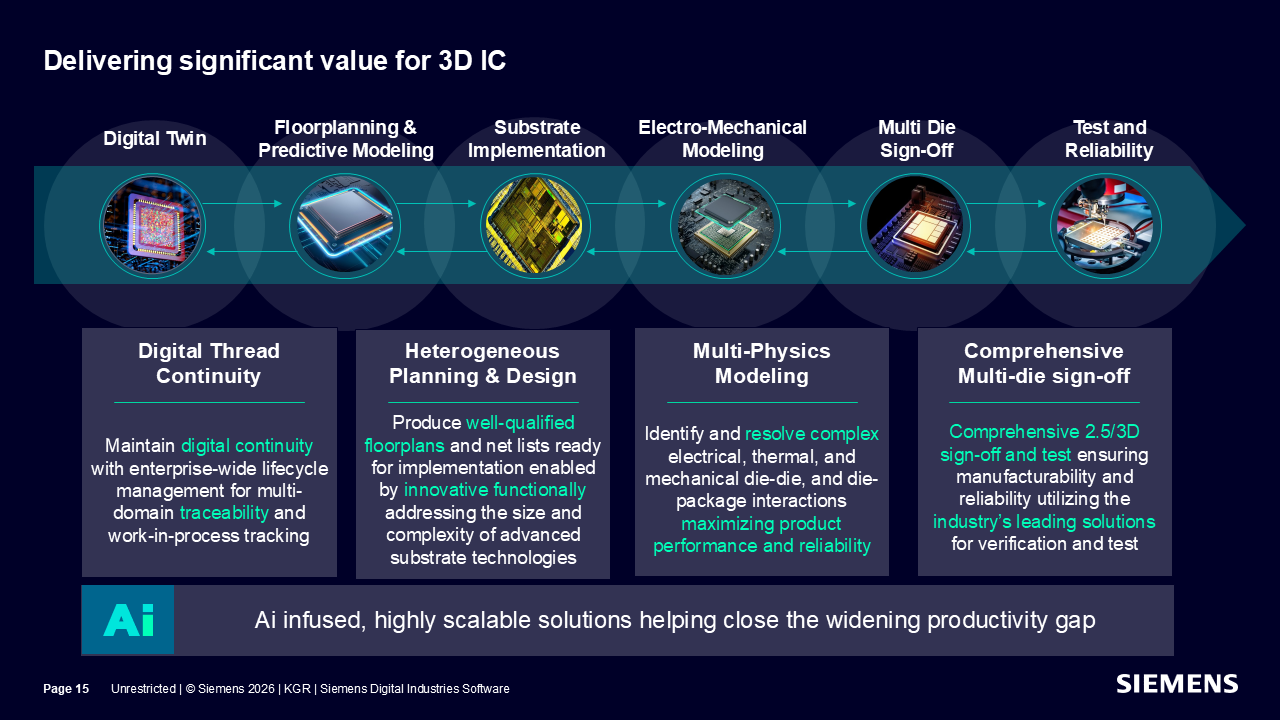
With our AI-powered, end-to-end 3D IC solution, Siemens maintains a digital thread from initial planning to final sign-off to ensure your design intent is never lost in translation.
The transition to 3D IC design solutions is no longer a matter of if, but when. For any organization driving the future of AI and HPC, the monolithic die is a closed chapter. 3D IC and the chiplet-based design—heterogeneous, stacked and hyper-connected—is the way forward.
The pillars of digital continuity
Our integrated workflow bridges the productivity gap through four critical capabilities:
- Digital thread continuity: Enterprise-wide lifecycle management with multi-domain traceability.
- Heterogeneous planning & design: Innovative functionality that produces well-qualified floorplans, regardless of complexity.
- Multiphysics modeling: The power to identify and resolve thermal and mechanical interactions before they become costly failures.
- Comprehensive sign-off: Industry-leading verification and test solutions to ensure manufacturability and long-term reliability.
Your competitive advantage: Confidence in complexity
The leaders of the next decade will be those who align strategy with execution today. By building a unified data foundation and embracing an AI-infused workflow, you move beyond experimentation and start delivering the high-performance systems that will transform our world.
Complexity is the new reality of semiconductor design. But with the right orchestrator, complexity doesn’t have to mean risk. It can mean competitive advantage.
Are you ready to scale? The tools, the intelligence and the workflows are here. It’s time to turn 3D IC potential into measurable business value.
Dive deeper:https://www.siemens.com/en-us/products/innovator3d-ic/
FAQs
Q1: How does Agentic AI improve 3D IC design space exploration?
A: Agentic AI uses autonomous software agents to control tools like Innovator3D IC and Calibre, simultaneously evaluating thousands of placement, thermal and SI scenarios to explore complex trade-offs far beyond human experience alone.
Q2: What is “data chaos” in 3D IC design, and how does a digital twin solve it?
A: Data chaos happens when IC designers, package engineers, and thermal experts work in isolated silos, passing disparate file formats back and forth. This manual hand-off process loses critical context and breeds errors. A digital twin acts as a persistent, unified orchestrator—a single source of truth that aggregates data across all levels of abstraction so every stakeholder collaborates on the exact same virtual model from day one.
Q3: How does Innovator3D IC Integrator bridge the gap between thermal management and IC design?
A: Innovator3D IC serves as a multi-domain collaboration cockpit. It allows teams to bring in power data as early as the VHDL description stage and assign real-world material properties (following JEDEC standards) directly to the assembly. Automated wizards handle complex calculations—such as thermal interface material (TIM) thickness—while reduced-order models enable secure, IP-protected sharing of critical thermal data with board-level teams without exposing proprietary floorplans.
Q4: What is the difference between AI-assisted tools and AI-driven design space exploration?
A: AI-assisted tools (available today) accelerate discrete, repetitive tasks, such as automated routing, predictive thermal modeling, and optimization of placement and verification workflows.
AI-driven exploration (emerging next) involves agentic AI systems that can coordinate workflows across multiple tools, evaluate thousands of competing trade-offs (power, performance, area, thermal, and signal integrity) simultaneously, and assist engineers through complex design spaces.
Q5: How does early multiphysics analysis help mitigate business risks in heterogeneous designs?
A: In the era of chiplets and 3D ICs, late-stage engineering changes are expensive business risks that can delay product launches. By performing predictive multiphysics analysis—evaluating mechanical stress, warpage, and thermal hotspots during the early floor-planning phase—teams can identify and fix failures when they are cheapest to solve, ensuring a well-qualified design ready for manufacturing handoff.
Q6: Why are multiphysics modeling and sign-off critical for 3D integrated circuits?
A: Unlike traditional monolithic dies, 3D ICs stack multiple chiplets and layers where heat, mechanical stress, warpage and signal integrity interact closely. Multiphysics modeling allows teams to predict thermal hotspots, creep strain and crosstalk early in the floor-planning stage, preventing costly late-stage respins.
Q7: What role does the Digital Twin play in heterogeneous integration?
A: In heterogeneous integration, the Digital Twin acts as a virtual, data-rich orchestrator representing the entire system—from individual chiplets and bridges to the interposer, package and PCB. It enables teams to perform predictive analysis, streamline collaboration and maintain a continuous digital thread from logic capture through final sign-off.
Q8: How does Siemens’ workflow support shift-left verification for high-speed signal integrity?
A: Siemens’ workflow enables protocol-aware validation (such as uCIE) and pre-layout analysis as early as the VHDL description stage. This allows designers to co-optimize channel structures, power data and equalization techniques before the physical layout is frozen, mitigating signal degradation and crosstalk early in the design cycle.