Scaling 3D IC design: Trends, challenges and practical workflows

Part 1: The reticle limit, advanced packaging and the multiphysics challenge
Authors: Kevin Rinebold and Andras Vass-Varnai, Ph.D.
This blog is the first of a two-part series distilling critical insights from a recent Siemens webinar featuring Siemens experts Kevin Rinebold and Andras Vass-Varnai, Ph.D., along with Brendan Burke, Research Director, Futurum Group, with datapoints provided by Futurum Research. Together, they explore the shift to heterogeneous systems and provide a blueprint for navigating this new era of 3D IC design.
Key takeaways: At a glance
- The challenge: As Moore’s Law approaches its physical limits and demand for compute power continues to rise, the era of the monolithic die is coming to an end, accelerating the industry’s shift toward chiplet-based and heterogeneous design
- The solution: System technology co-optimization (STCO), enabled by shift-left multiphysics analysis, is becoming essential for addressing thermal, power and integration bottlenecks in advanced-node and multi-die designs
- The tools: Siemens Innovator3D IC and Calibre 3D IC products provide an integrated die-package-system co-design workflow with predictive multiphysics analysis to help teams plan, optimize and implement 3D IC systems effectively
The transition to 3D IC is no longer a future concept, it is the architecture of now for AI, high-performance computing (HPC) and advanced semiconductor systems. As we move from monolithic dies to advanced packaging systems, the design rules are being rewritten for a heterogeneous future. Welcome to the era of 3D IC and chiplets. Scaling these designs introduces new challenges in connectivity, thermal management, signal, power and mechanical integrity.
Whether you are an IC designer, a package engineer or a systems architect, by the end of this blog series, you will have gained:
- Strategic market insight: Understand the industry drivers making 3D IC the standard for AI and HPC
- A multiphysics blueprint: Learn to move beyond siloed design by addressing thermal, power and connectivity challenges concurrently
- The power of the Digital Twin: See how a unified approach allows for die-package-system co-design, reducing late-stage risk and accelerating time-to-market
- Compelling AI design insights with Andras Vass-Varnai, Ph.D. who remarks,“We are moving toward AI-based intelligence to simplify and automate the creation of multiphysics flows… providing insights that exceed human experience alone.”
- A practical path forward: Walk through an integrated workflow using Siemens Innovator3D IC to turn 3D IC potential into a scalable reality
What is advanced packaging design and the reticle limit?
The main problem is that you cannot keep shrinking transistors, as lithography and transistor sizes reach a physical limit, or at least the price of going smaller exponentially increases even if it is possible. We also cannot make the chips larger as the reticle size is a hard limit, therefore the solution is to add more chiplets into a package and integrate them tightly. There is no super chip, but a package can host a lot of chips (chiplets – a chiplet is a chip designed for integration), with this still increasing compute power in a more scalable way.
As Brendan Burke, Research Director at Futurum, describes it:
“The reticle limit of 858 square millimeters means that you cannot pattern a monolithic die larger than it… So, the answer became…many chiplets integrated to behave as one system, and the package became the thing that actually scales.”
Why have we reached the end of the monolithic die?
The shift to advanced packaging systems represents a shift in how computing systems are designed and integrated. In the past, we tried to cram everything, including logic, memory and input/output (I/O) onto a single, monolithic piece of silicon. As AI models explode in size, the hardware required to run them has outgrown the surface area we print it on.
So, instead of one giant, expensive die, we are breaking the system down into chiplets. This allows us to mix and match process nodes, using the most advanced available process technologies for compute-intensive functions. We are integrating high-bandwidth memory (HBM) closer to the compute fabric, reducing data travel distance and increasing bandwidth.
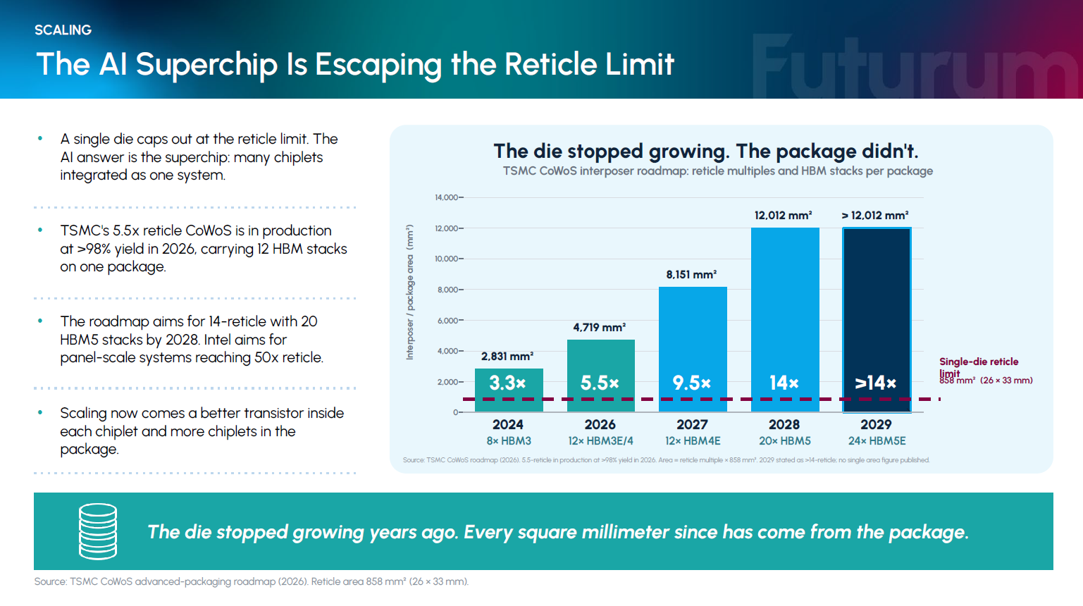
According to Burke, TSMC’s roadmap moves from a 5.5-reticle CoWoS package in production today at greater than 98% yield with 12 HBM stacks on a single package toward larger multi-reticle implementations with significantly more HBM capacity. By 2028, it will reach 14 reticles with 20 HBM5 stacks and will keep growing.
What is the shift from designer to architect?
This shift affects both engineering workflows and organizational structures. Today’s IC designers face a broader set of responsibilities than previous generations. You are no longer just responsible for the gates and wires on a single die. Designers now need to think like systems architects.
Engineering teams now manage a complex ecosystem where the boundaries between the chip, the package and the board have blurred. In this new world, the package is no longer just a protective shell. It is the platform where scaling happens.
Why are there three integration pathways?
The industry is pursuing three integration answers in parallel, because different compute workloads hit different walls, particularly in terms of memory integration.
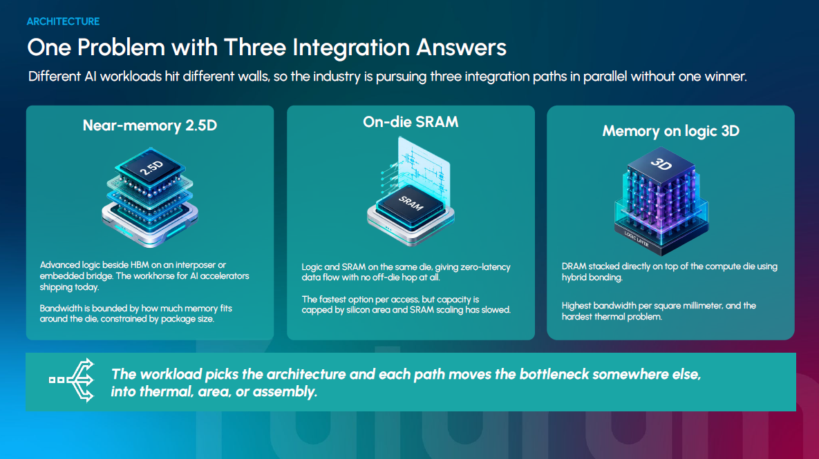
Burke: “There is no one single winner. Near-memory 2.5D is the workhorse of today’s AI accelerators. By placing logic beside HBM on an interposer or embedded bridge, it powers nearly every accelerator on the market. However, its bandwidth is strictly limited by the physical geometry of the die. On-die SRAM is fast but scales poorly, consuming more expensive die area every generation. 3D memory stacking offers a high bandwidth memory (HBM) alternative but introduces thermal risks by placing DRAM next to the hottest logic.”
In 3D IC, you don’t eliminate bottlenecks—you choose where to shift them. Every design decision is a trade-off between thermals, area and assembly complexity.
What is the multiphysics challenge?
When you move from a flat, 2D chip to a stacked 3D architecture, you aren’t just adding a third dimension, you are creating a tightly coupled physical system, where thermal, electrical and mechanical effects interact continuously. In a traditional design, heat and power have plenty of room to spread out. In a 3D stack, they are trapped.
The challenges of thermal management, power delivery and mechanical stress are no longer secondary concerns. They are the design.
The vertical thermal challenge
Stacking active silicon creates a critical thermal bottleneck: Heat from the lower die must dissipate through the layers above it. If these thermal paths aren’t optimized during the initial floor-planning stage, the system risks failure from overheating upon power-up. In 3D IC, thermal analysis can no longer be a final “sign-off” task. Waiting until the end of the cycle to identify a hotspot often results in a total redesign, as vertical thermal failures are nearly impossible to patch in a finalized stack.
The cost of complexity
Scaling introduces additional thermal, power-delivery and mechanical-design constraints.
When you stack dies and crowd chiplets together, you create a “high-pressure environment” where every design choice has a ripple effect.
“Every step makes the physics harder,” Burke warns, “because you get more thermal coupling, more IR drop, more mechanical stress, and all of that has to be managed concurrently.”
Back in the monolithic days, you could solve for power, then move to signal integrity, then check your thermals. In the era of advanced packaging, you no longer have that luxury. If you move a chiplet to solve a routing issue, you might accidentally create a thermal hotspot that cracks the microbumps.
The why of 3D IC is clear: It’s the only way to keep up with the AI revolution. But the how requires a new way of working, where physics and design are no longer separate conversations.
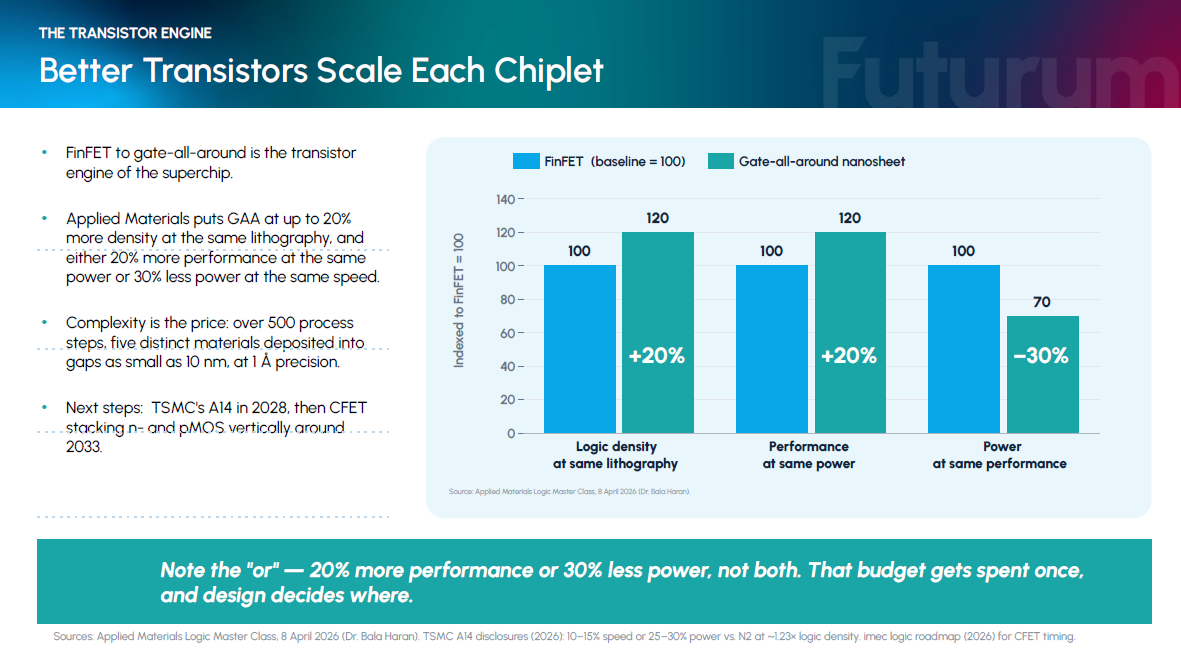
Burke warns, “It’s a trade-off between performance and power. Compared to a Fin Field Effect Transistor (FinFET), Gate-All-Around (GAA) technology offers a 20% density boost, but it comes with a choice: 20% more performance or 30% less power. You can’t have both. In 3D IC, your design decides which one you get.”
Why does design matter more now?
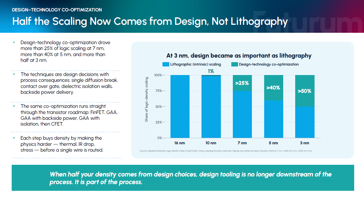
As Burke puts it, “For 40 years, lithography was the primary driver of chip density. Today, that has flipped. System technology co-optimization (STCO) now contributes over 50% of logic density gains at 3nm. This means density is no longer just a ‘process’ outcome—it is a design decision.”
Engineers are now gaining density through architectural innovation—like vertical stacking—rather than just node shrinks. This shift requires managing heat, power and stress during early floor-planning, making architecture the primary lever for performance.
The power delivery challenge
Delivering clean, stable power to the center of a 3D stack is a critical hurdle. As die-count increases, wiring resistance skyrockets, causing traditional power delivery methods to fail. Designers must now account for multi-layer IR drop (voltage drop) from the very start, ensuring the logic at the core receives sufficient power without overheating the surrounding circuitry. Because these physical constraints are so severe, you cannot wait for sign-off to check them. Instead, you must analyze the power and thermal impact during the initial design phase.
What is system technology co-optimization (STCO)
STCO is a comprehensive approach that integrates process technology decisions, standard cell architecture, library development, and design methodology co-optimization to enhance semiconductor performance, manufacturability and efficiency.
STCO has become a critical industry methodology for maximizing scaling benefits. At the system level, similar co-optimization principles can be extended into architecture, floorplanning, thermal management and package design.
STCO helps teams evaluate tradeoffs across power, performance, manufacturability and thermal behavior earlier in the design process.
The organizational challenge: Breaking down silos
The challenge of 3D IC multiphysics is both technical and organizational. Traditionally, thermal, package and IC teams have worked separately, leading to fragmented communication and inefficient workflows. To succeed in 3D IC design, these silos must be eliminated. A shared framework is essential for early evaluation of thermal, mechanical and electrical trade-offs, while collaborative co-optimization fosters better decision-making across disciplines.
What is making a material difference?
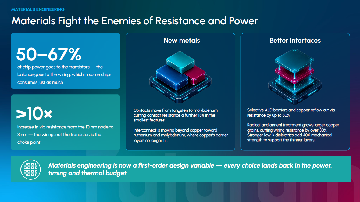
Burke: “The 2,000-mile choke point refers to the fact that a leading-edge AI GPU contains 300 billion transistors and over 2,000 miles (3,200 kilometers) of copper wiring. As we scale to 3nm, this wiring has become a critical choke point, with resistance rising tenfold. Designers can no longer treat wiring as ‘free,’ as it now consumes up to half of the total chip power.”
How do you scale up and out?
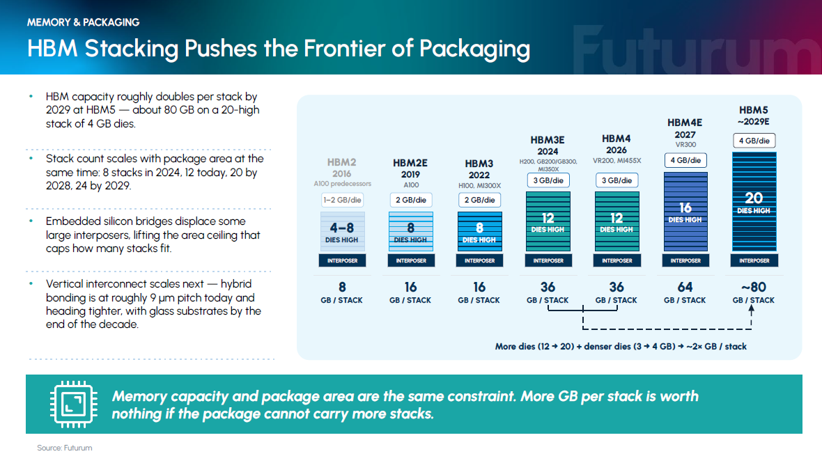
Burke predicts that “HBM capacity is set to double, reaching 80GB on 20-high stacks. But the real story is connectivity. To build the next generation of advanced packaging systems, designers are using horizontal silicon bridges and vertical hybrid bonding to unite disparate chiplets on a single substrate and then using alternative substrates to combine these multiple types of chiplets together. This multi-layer approach allows for denser, more integrated architectures that push the limits of both memory and compute.”
Memory capacity and package area
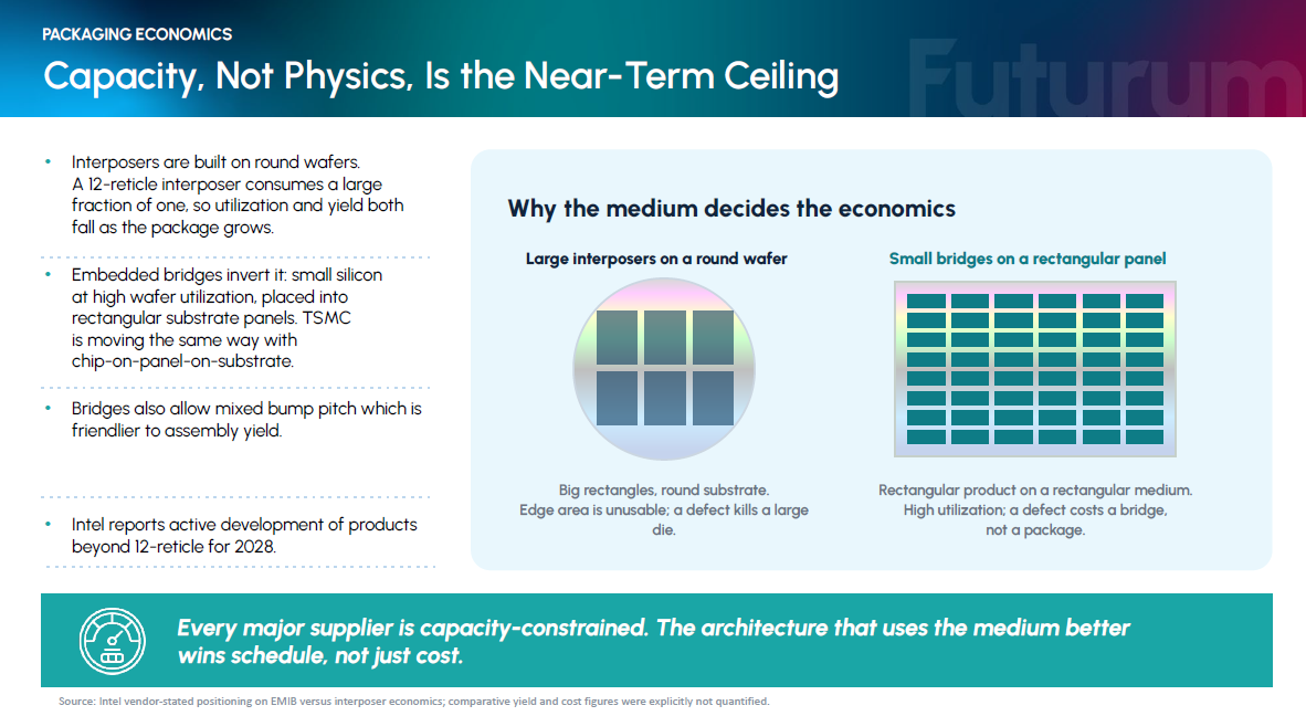
Burke: “Every major supplier is currently capacity constrained. The winners will be those who use their manufacturing medium most efficiently. By switching from large interposers on round wafers to small silicon bridges on rectangular panels, manufacturers can protect their yield and accelerate their schedules, turning packaging economics into a competitive advantage.”
What is shift-left multiphysics design?
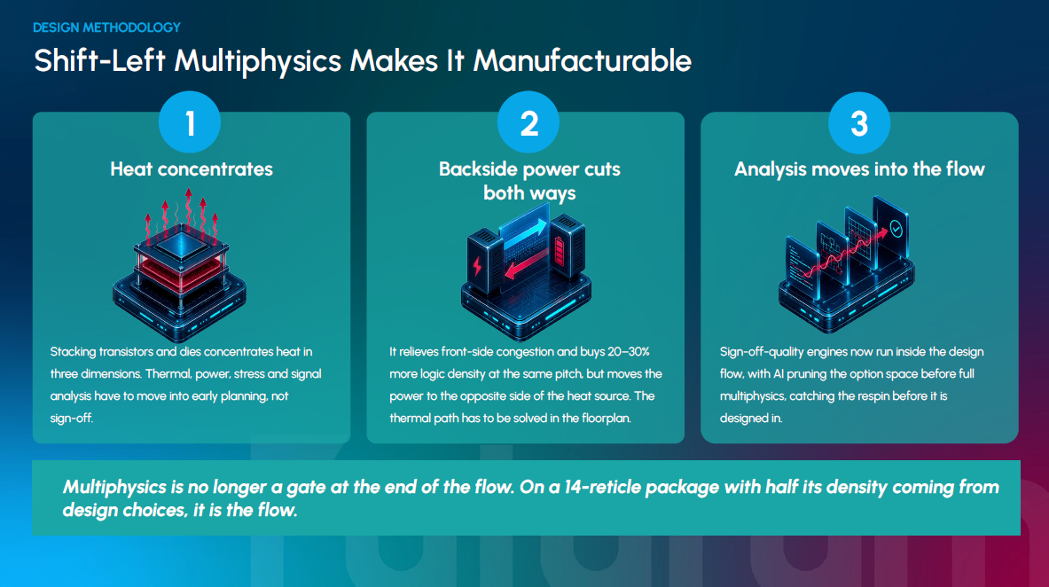
According to Burke: “By shifting left, designers are turning multiphysics into a design advantage. That is because in 3D IC, multiphysics is no longer a final gate—it is the design flow itself. By ‘shifting left,’ designers can solve for heat concentration and power delivery early at the floor-planning stage.”
Addressing these thermal, power and packaging challenges requires more than individual point tools. Engineering teams increasingly need workflow integration across IC, package and system design domains. In Part 2, we will examine how a digital twin approach and Siemens Innovator3D IC support shift-left multiphysics analysis and AI-driven design space exploration.
Meanwhile, explore more at www.siemens.com/en-gb/company/electronic-design-automation/trending-technologies/3d-ic-design/
FAQs
Q1: What is advanced packaging and why is it important for AI?
A: Advanced packaging enables the integration of multiple chiplets, dies, and memory components into a single package designed to function as a high-performance computing platform. As AI and high-performance computing workloads continue to expand, advanced packaging helps surmount the size limitations of monolithic dies while allowing for increased compute density, memory capacity, and scalability.
Q2: What is the reticle limit in semiconductor design?
A: The reticle limit refers to the maximum area that can be patterned on a single piece of silicon during lithography. Because advanced AI processors increasingly require more transistors and memory than can fit on a single die, designers are turning to chiplet-based architectures and advanced packaging technologies to continue scaling performance.
Q3: Why is thermal management more challenging in 3D IC design?
A: In 3D IC architecture, multiple layers of active silicon are stacked vertically, creating more concentrated heat sources and more complex thermal paths. Heat generated in lower dies must travel through upper layers, making early thermal analysis critical to avoid hotspots, reliability issues and costly redesigns.
Q4: What is system technology co-optimization (STCO)?
A: STCO is a comprehensive approach that integrates process technology decisions, standard cell architecture, library development, and design methodologies to enhance semiconductor performance, manufacturability, and efficiency. By leveraging these co-optimizations, engineers can address the challenges presented by advanced technology nodes, ensuring scalable solutions that meet demanding market requirements.
STCO has become a critical industry methodology for maximizing scaling benefits. At the system level, similar co-optimization principles can be extended into architecture, floorplanning, thermal management and package design.
Q5: Why is shift-left multiphysics analysis important for 3D ICs?
A: Shift-left multiphysics analysis moves thermal, power-delivery and mechanical-impact evaluation earlier in the design process. By identifying potential issues during floor planning, engineers can eliminate problematic design options sooner, improve manufacturability and reduce the risk of expensive design re-spins.
Q6: How do chiplets enable scaling beyond traditional monolithic designs?
A: Chiplets allow designers to partition functionality across multiple smaller dies that can be combined in advanced packages. This approach supports heterogeneous integration, improves manufacturing flexibility and enables teams to mix process technologies, memory and specialized compute functions within a single system.