User2User 2024: Advanced physical verification flows for 3D IC’s
In this User2User 2024 video presentation, now available on-demand, Microsoft’s Amit Kumar discusses 3D IC verification flows with a focus on physical verification. This session explores how 3D ICs enhance system performance and compactness – but challenge verification with their complex tech layers. Amit also discusses methodologies, standards, and solutions, including Siemens XSI & Calibre 3DSTACK uses.
An introduction to the basics of 3D IC
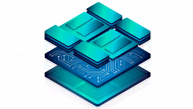
Amit describes how the architecture of three-dimensional circuits allows chips to be stacked vertically. Depending on the technologies being used, the connections between components require connections like TSVs (through silicon vias) and hybrid bonding. 3D ICs are already widely used for networking, mobile and GPUs. They enable heterogeneous integration and are now being leveraged for emerging technologies, including MEMs and photonics.
What are the advantages of 3D IC?
- Reduced cost and footprint
- Higher bandwidth
- Lower power consumption
- Heterogeneous integration
What are the challenges of 3D IC?
- Overall system cost is higher
- Yield is lower for the whole system
- Higher power density and reduce heat dissipation
- Design complexity – cross die-placement and routing
- TSV overhead
- New sources of timing variations due to TSV’s
- Require new testing and verification methods
- Needs to support hierarchical and modular approaches
- Lack of standards
Flow and data management challenges in 3D IC
In a traditional IC flow, you have to deal with only a few things when you develop from RTL to GDS. For 3D IC you are dealing with multiple flows together in the same timeline.
You have to work with different teams, different engineers, you have to enable different flows that enable the whole system starting from the die and different components
Amit Kumar – Principal Hardware Engineer -Microsoft
Effective data management is crucial for successful system design, especially when dealing with multiple stakeholders and intricate processes.
- Die-level and component-level specs: Your internal team generates specifications for the die-level and component-level based on the overall system design.
- Tech files and collateral: Depending on whether you work with a foundry or an OSAT, you gather all relevant tech files and collateral.
- Third-party integration: If you use third-party ICs or chiplets, you integrate them into your system. This involves understanding their specifications, bump locations, and other details.
- Complexity and parallel work: Managing these diverse data elements adds complexity. To “tape out”, you coordinate with different teams. This often requires parallel work rather than a sequential approach, which can be challenging due to tight timelines.
An introduction to TSMC 3DBlox 1.0 and 3DBlox 2.0
Amit also describes the focus on and evolution of 3DBlox 1.0 and 2.0 standards. These standards are available via an open-source standards committee of which many EDA vendors and other companies are working with TSMC and help describe the steps needed to perform analysis and verification while taking into account EDA vendor-to-vendor tool compatibility. 3DBlox 2.0 introduced added pre-analysis functionality, as once you build a system or move your bump, for example, at that point, it will be too late. Amit presents the results of an experiment using 3DBlox in their Microsoft environment in this video.
Physical verification and reliability analysis for 3D IC
On the 3D IC physical verification side, the focus is mainly on DRC, ESD, connectivity and alignment to ensure all those things are correct. ESD is especially critical because it’s being done at the die level, the SoC level, to perform point-to-point and current density checks. Amit states there is more work needed on this front.
The approach to 3D IC verification: Amit states that typically, when we try to build everything, we start with the bumps. Sometimes, we get bumps from the foundry, and sometimes, we create our own bumps. So, we create a bump library, basically different configurations with the proper pads and everything – then, using those bumps from the bump library, we do SoC planning. Amit provides an in-depth walk through a verification flow that includes:
- uBump library and delivery flow
- Die level, package, and interposer verification.
- Physical verification using XSI and Calibre 3DSTACK.
- Optical shrink and thermal expansion handling
Microsoft: Looking ahead at 3D IC
The advantages of 3D IC enable Microsoft to generate low-power, high-performance, high-bandwidth chips in a 3D manner via vertical stacking. Though there are many challenges and work that needs to be done, Microsoft is working with the foundry and end vendors to develop some of the solutions for Microsoft and the broader 3D IC design ecosystem. That said, Amit states that the industry needs standardization that is not exclusively from TSMC. According to Amit, “I think it should go beyond any foundry; it should be for the general ecosystem.”
If you missed User2User 2024 or attended the event and want to watch the 3D IC sessions again, the library of videos is now available on-demand here: Click here
To learn more about Siemens EDA 3D IC solutions, visit our 3D IC Homepage


Comments
Leave a Reply
You must be logged in to post a comment.
I appreciate how this perspective invites deeper thinking about the subject. Solar