A touchy subject: RF IC layout verification

By Neel Natekar
Radio frequency (RF) circuitry is an essential component of many of the critical applications we now rely on every day, including cellular communications, global positioning systems (GPS), the Internet of Things (IoT), and transportation electronics. However, as every circuit verification engineer knows, RF circuits can be, well, a bit touchy when it comes to parasitics and layout-dependent effects. Both pre- and post-layout simulations must be used to ensure the final results is a robust circuit that will operate reliably in a wide range of conditions.
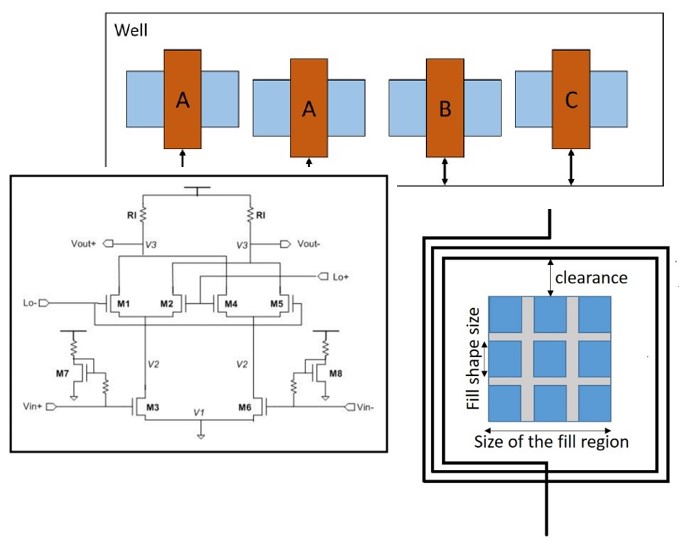
On the downside, those simulations, particularly at the full-chip level are resource-intensive and time-consuming. While we can’t eliminate them altogether, there are ways to reduce the number of simulation iterations required. Selective verification strategies enable designers to verify and debug device type, device properties, orientation, symmetry, and other critical design parameters in RF circuits. Because both the performance and reliability of RF designs are closely linked to the layout implementation, finding and eliminating these impacts on reliability and performance go a long way towards ensuring the accuracy of the design before moving on to simulations.
But it isn’t just these design parameters designers have to consider. Fill can also negatively affect the performance and yield of RF designs. The potential effects of fill on resistance, capacitance, inductance, and resonant frequency make it critical to optimize the fill process. Such factors as consistent fill placement, sufficient clearance of fill shapes from the critical nets, and determination of the optimum fill shape size can help maximize performance, minimize the interconnect losses, achieve the desired Q-factor and resonant frequencies for inductors, and improve yield.
Leveraging the advanced verification functionality of the Calibre PERC reliability platform to automate complex verification processes within every stage of the design, and using an amalgamation of Calibre tool functionality to standardize and optimize post-layout fill insertion, RF IC designers can drastically reduce overall verification time while still ensuring their designs will perform reliably over the lifetime of the products in which they are used.
To get the details, download a copy of our technical paper, Improving the reliability and performance of RF ICs with advanced EDA technology. If you like what you read, contact our team for a software evaluation, and start optimizing that simulation workload today.


