ECO Fill Can Rescue Your SoC Tapeout Schedule
By Vikas Gupta and Bhavani Prasad, Mentor Graphics
Automated ECO fill helps you refill and re-verify late-stage changes quickly, while avoiding mask respins
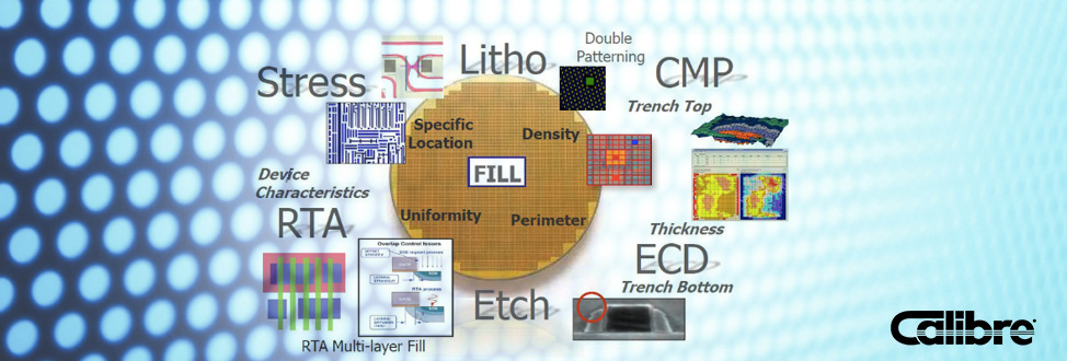
Integrated circuit (IC) design and manufacturing is one of the most challenging engineering industries. As soon as a design engineer gets into “the groove” and feels comfortable taping out in a particular technology node, the next technology node shrink is already there to pose a new and greater set of challenges. While it almost goes without saying that design rules and design rule checks (DRC) become increasingly complex as the industry moves to the next node [1], at the same time, dummy fill requirements have also undergone a great deal of transformation (Figure 1).
Figure 1. Expanding manufacturing needs drive increasingly complex fill requirements.
Dummy fill insertion for every layer of IC fabrication is a mandatory requirement to enable flawless and robust manufacturing. One of the most important manufacturing requirements is to meet required density criteria in a specified window of an integrated circuit (IC) layout. This density criterion helps produce a planar surface after the chemical-mechanical planarization (CMP) manufacturing process, which is critical to ensure proper manufacturing of the next layer on top. The specified window size and spacing varies with every process. However, for advanced technology nodes, it is no longer adequate to meet the minimum density value in a single specified window. Designers must make sure that the density gradient across neighboring windows is also within acceptable margins. From a manufacturing standpoint, dummy fill insertion also improves the results of other manufacturing processes, like rapid thermal annealing (RTA) and uniform etch loading.
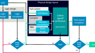
Fill and ECOs
System-on-chip (SoC) integration is a parallel activity to the development of the intellectual property (IP) for an SoC, and multiple revisions of IPs are usually delivered to the SoC integration team during project development. However, as the full-chip integration team approaches the final iterations, the expectation is for a minimal set of changes. At this stage, any engineering change order (ECO) that requires a change to the metal routing means the integration team has no option but to remove the existing fill and re-do the fill insertion. In addition to being time-consuming, significant modification to already inserted fill geometries can have an undesirable impact on the timing analysis closure done during the previous stage. Further, the full chip integration team has typically converged to compliance with complex density requirements at this stage. Complete regeneration of fill triggers another wave of timing and density validation, with high uncertainty as to the results, and could jeopardize project schedules. Meeting both timing and fill requirements is a design challenge that, once achieved, you want to protect against any impact from late changes. What is needed is a balance between using the plan of record fill deck from the foundry and the need for an ECO fill solution.
So, what can we do? The most efficient way to handle such a scenario is to surgically change fill geometries in the neighborhood of ECO changes, while keeping the rest of the geometries intact. This approach not only requires less time to fill a smaller area near the ECO region, but also preserves other metrics of timing closure and density validations. Let’s walk through an ECO fill process.
The ECO Fill framework (Figure 2) requires four inputs:
- Reference Design: Original design layout before any changes are made
- ECO Design: Design layout that incorporates changes required by ECO
- Reference Fill: Fill layout as done on original design layout
- Calibre SmartFill rule deck and technology library: Required to re-fill as needed.
The output of the ECO Fill framework is an ECO fill layout, which can be directly used with the ECO design layout.
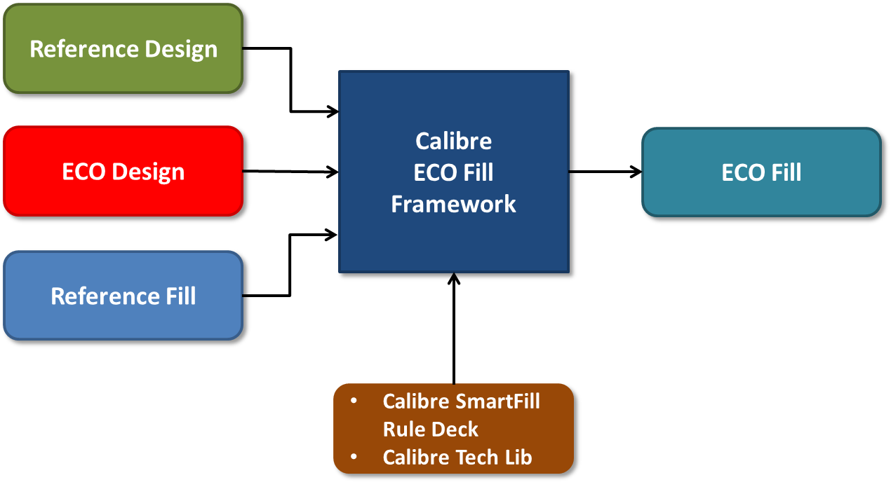
Figure 2. Calibre ECO Fill Flow Methodology
The Calibre SmartFill utility automatically uses the reference and ECO design layouts to identify those regions/layers where changes have been made. These identified regions are the locations where the ECO Fill process will surgically add/remove fill shapes. Any layout locations where the original design layer was moved now contain empty space. These locations can be re-filled using a regular Calibre SmartFill rule deck. Layout locations where a design layer has been added now contain overlapping fill shapes. These fill shapes are deleted selectively by preserving as much hierarchy as possible. There is also a “no refill” option available, in cases where the designer only needs to remove fill shapes. Figure 3 illustrates the ECO fill process.
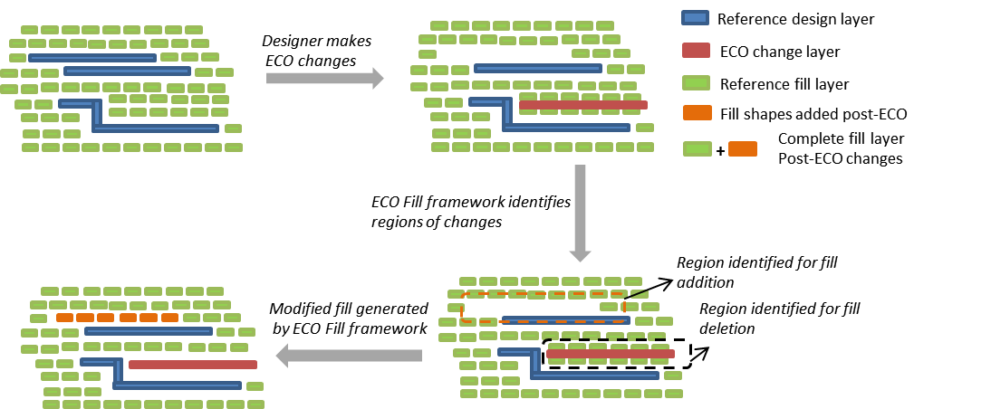
Figure 3. ECO fill flow process
The ECO fill process works best when design changes are minimal, which is the expectation for final tapeout changes. In the case of major changes to a layout, designers should typically re-fill the design, as the new layout will probably require re-verification.
Conclusion
Overall requirements to meet tapeout criteria are increasingly complex, while project schedules remain pretty much unchanged, creating aggressive time-to-market goals. Management of complexity and capacity requirements is being pushed into CAD teams. Using an automated ECO fill process during SoC integration stages can significantly reduce verification time while providing optimized results. SoC integration engineers can see immediate benefits, not only with respect to faster runtimes, but also minimal/zero complexity during timing closure and density corrections. An automated ECO fill process is also helpful for full-chip ECOs post-silicon validation, where designers want to avoid a major churn in their layout. From a manufacturing/fab perspective, the ECO fill process helps change a minimal set of layers, which can help reduce mask costs.
While the ECO fill process was first developed for advanced technology nodes like 28nm and below, it can be a useful methodology for older nodes, as well. If you struggle to implement ECOs while meeting your tapeout dates, perhaps an automated ECO fill process can help you regain control of your schedule while ensuring quality of results.
References
[1] White. Michael. “Are You (Really) Ready for Your Next Node?,” Electronic Design. Jan 4, 2017.
Authors
Bhavani Prasad is a senior application engineer for physical verification in the Design to Silicon division of Mentor Graphics
Vikas Gupta is an applications engineering manager for Physical Verification and AMS in the Design to Silicon division of Mentor Graphics

Liked this article? Then try this –
Blog: Are You (Really) Ready for Your Next Node?
This article was originally published on www.semiengineering.com