A new path for analog design constraints verification
By Dina Medhat, Mentor Graphics
Accurate verification of explicitly-defined analog design constraints is crucial for reliability and performance.

Design constraints describe and define an IC’s performance intent. For example, electrical and thermal design constraints are specified and then transformed into physical constraints for layout to ensure those domains perform as intended. Physical layout constraints can also be derived from circuit patterns or extracted layout netlists.
Given all that, it follows that the verification of design constraints is of utmost importance to guarantee the resulting function of a final physical IC matches the performance intent. For analog and mixed-signal (AMS) design there is a growing need for this verification process to take place during a project’s design phase.
Consistent evaluation of design constraints and automatic constraint verification are two highly effective ways of addressing design standards (e.g, the ISO 26262 automotive standard). Today’s shortening innovation cycle exacerbates the AMS verification challenge, as design engineers find they often cannot rely on their experience of proven concepts or components as they did at earlier process nodes. As a result, design engineers must increasingly turn to explicitly defined design constraints to describe design intent and predefine design limits set by the target process technology and IC specification.
Design constraints for analog circuits take different forms from those for digital ones. AMS circuitry is very sensitive to changes in environmental conditions, technology variations, and various aspects of the manufacturing process. The last of those can have a negative impact on device matching (e.g., well proximity and stress effects) or on circuit robustness in general. Because individual constraints typically span multiple hierarchy levels, they must be fully considered and verified in that context.
Typical constraint types (also shown in Figure 1) include:
- Alignment: Alignment is a constraint that is not necessarily quantitatively relevant for matching, but often expected for a good layout arrangement. It requires members to be on the same alignment edge with their x or y
- Symmetry: Symmetry can be enforced for either one or both axis directions (e.g., it is important for common centroid arrangements).
- Matched device orientation: Matched orientation is a constraint that protects against global variation gradients, including mask misalignment or crystal orientation. Assuming a well-defined orientation vector for each member, this constraint requires that these vectors have either the same angle or opposite angles.
- Matched device parameters: Parameter value matching is a well-known constraint criterion used as a pre-condition for the proper layout implementation of matching devices from unit devices. In a basic implementation, it can be checked at the netlist/schematic level (e.g., ensuring equal length of matching MOS transistors). In an advanced implementation, constraint semantics are extended to cover parameter values extracted from the layout.
- Cluster: Clustering devices to keep them in a common area without disturbing other nearby devices is a basic matching constraint. Clustering can be used for robustness against global variation gradients, including thermal influence. Designers define clusters generically by an automatically created common outline (hull) of their members. This hull can be extended by a specific distance (halo). A violation of a cluster constraint occurs when other instances either cross the hull or lie within the hull.
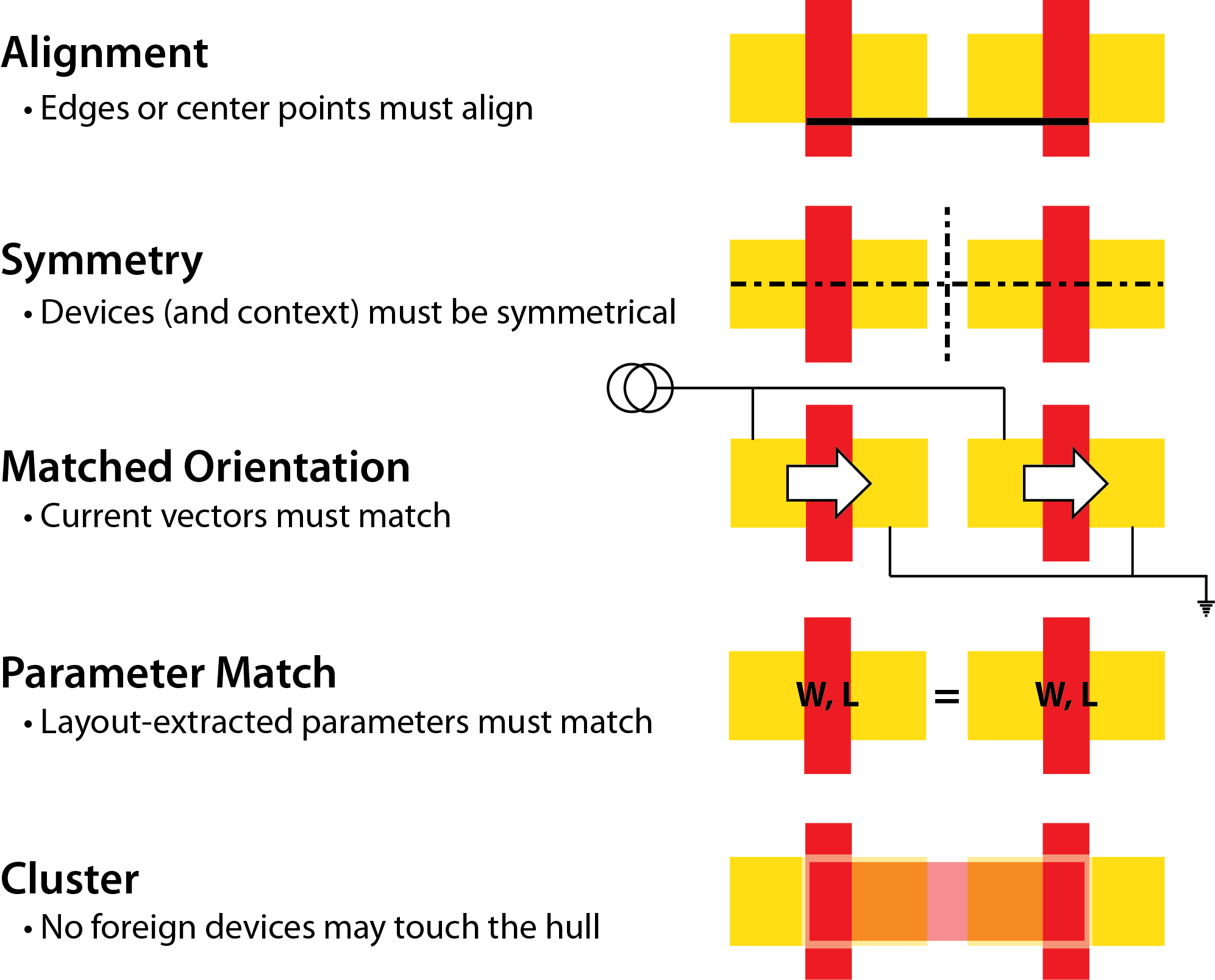
Figure 1. Typical analog design constraints (Mentor Graphics)
Constraints verification flow
A comprehensive analog design constraints verification flow ensures the constraints are properly defined and implemented in a layout. To avoid typical errors (Figure 2a-2c), a modular and extensible industrial-strength automated verification approach must be able to:
- derive analog-focused design constraints from an existing circuit or extracted layout netlist; and
- verify analog constraints such as clustering, matched orientation, matched parameters, alignment, and symmetry across multiple design hierarchy levels.
This verification flow must then perform two primary functions.
- It must assign sets of predefined constraints to automatically-recognized hierarchical circuit structures found in either existing schematic netlists or extracted layout netlists. By employing a circuit pattern recognizer, this technique can also be used to verify existing IC designs without the need to explicitly define constraints.
- It must verify the compliance of a physical layout with respect to its assigned hierarchical constraints.
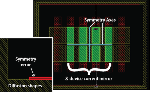
Figure 2a. Typical analog constraint error: Symmetry error on diffusion context (Mentor Graphics)
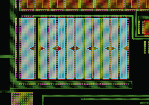
Figure 2b. Typical analog constraint error: Anti-parallel current vectors (Mentor Graphics)
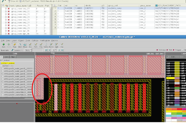
Figure 2c. Typical analog constraint error: Unmatched ‘delvto’ – inconsistent well proximity (Mentor Graphics)
Verification tools such as Mentor Graphics’ Calibre PERC reliability platform give designers unified access to all the relevant types of design data (i.e., physical, logical, electrical) in a single environment. This enables the automated evaluation of topological constraints within the context of physical requirements. By offering a flexible and extensible verification capability within an enhanced logic-driven layout (LDL) physical verification framework, Calibre PERC seeks to ensure the accurate physical implementation of design constraints in analog designs (Figure 3). It has been tested successfully on large industrial automotive IC designs for safety and electronic stability control applications, and has been adopted as a required component of multiple IC sign-off verification flows [1].
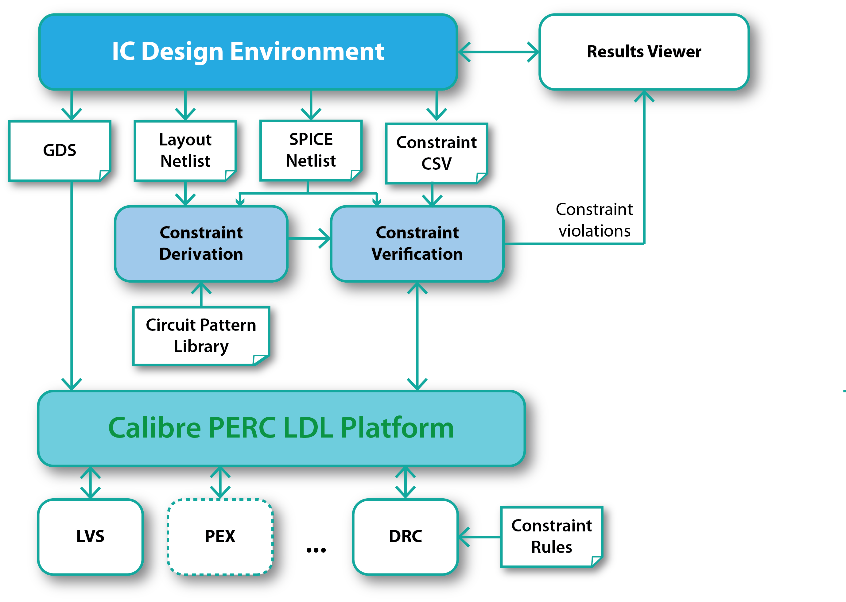
Figure 3. A constraint verification flow using the Calibre PERC reliability platform (Mentor Graphics)
Increasingly, analog design engineers use explicitly defined constraints to describe the design intent and to predefine design limits set by a target technology and IC specification. In the automotive market, the implementation of such design constraints alongside an automated process that combines physical, logical, and electrical design elements to accurately verify compliance provides an effective means of addressing ISO 26262 traceability requirements. Other industries with high reliability and strict performance requirements also benefit from the improved convergence between design intent and physical implementation.
References
[1] V. Meyer zu Bexten, M. Tristl, G. Jerke, H. Marquardt and D. Medhat, “Physical verification flow for hierarchical analog IC design constraints,” The 20th Asia and South Pacific Design Automation Conference, Chiba, 2015, pp. 447-453.
doi: 10.1109/ASPDAC.2015.7059047
Author
Dina Medhat is a Technical Lead for Calibre Design Solutions at Mentor Graphics. She has been with the company for 11 years. Dina holds a BS and MS from Ain Shames University, Cairo, Egypt.

Liked this article? Then try this –
Blog: Context-Aware Latch-Up Checking
This article was originally published on www.techdesignforums.com

Comments
Leave a Reply
You must be logged in to post a comment.
It is good to see articles such as this so well written and presented.
http://www.peakperformancesalestraining.us