IoT, Cost-per-Transistor Extend Lifetimes of Established Technology Nodes
By Michael White, Mentor Graphics
Much of the Internet of Things (IoT) functionality we crave is more cost-effective when implemented at established nodes between 40 nm and 180 nm…

Established nodes are experiencing a much higher demand than one might normally expect at this point in their lifecycle. We believe this is driven by a couple of market dynamics, as discussed below. Their extended lives have brought some interesting physical verification, design-for-manufacturing (DFM), and manufacturing challenges to those seeking to leverage the benefits of these established nodes.
Why are Established Nodes Experiencing a Long Life?
The appetite for faster, smarter, lower-power, more interconnected, data-rich computing among the advanced economies worldwide (e.g. Europe, Japan, China, U.S., etc.) becomes more voracious by the day. Basic computing power continues to be driven by more powerful application processors, CPUs, GPUs, microcontrollers, memory, etc. marching down the Moore’s Law path. The iPhone, GoPro, and Nest have application processors and memory implemented at advanced nodes, such as 20 nm or 28 nm.
However, much of the Internet of Things (IoT) functionality we crave, such as smart power management for longer battery life, and Wi-Fi and Bluetooth for more connectivity, are more cost-effective when implemented at established nodes between 40 nm and 180 nm. Consequently, the high consumer demand for these capabilities is driving demand for ICs manufactured using these processes. In a nutshell, the nodes that best support RF and mixed-signal IC designs with low power, low cost, and high reliability are experiencing much higher demand than in the past.
The other dynamic benefiting the long life of established nodes—40/45 nm and 32/28 nm in particular—is the wafer cost trends at 20 nm and below. As I have previously written, with the semiconductor capital equipment industry stuck at the 193-nm wavelength, the only viable strategy to maintain a reasonable K1 and continue pursuing Moore’s Law is the use of multi-patterning.
Multi-patterning at 20 nm and below has enabled further scaling, but the inherent process complexity has driven up wafer cost, changing how fabless companies look at the jump to the next node. Just a few years ago, the jump would have been nearly automatic. However, with the cost structure of 20 nm and below, companies must seriously consider whether sales of the next design will really justify investing in the next node.
We are seeing many companies make the jump to 20 nm, 16/14 nm, and 10 nm, but it tends to be those who are confident that they can sell in very high volumes while commanding premium average selling prices for their products. Also, the early adopters are companies that really need the advanced capabilities of the next node (e.g. high-end FPGAs, high-end application processors, CPUs, GPUs, memory, etc.) and feel they cannot be competitive at established nodes. However, more and more companies are finding that their business case doesn’t justify being an early adopter, and instead choose to stay at 28 nm and above.
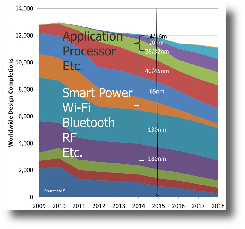
1. Design completions skew heavily toward established process nodes. (Source: VLSI Research)
With all of the media focus on advanced nodes, if you paid attention to press releases alone, you might conclude that most designs were at 20 nm to 14 nm. Therefore, this graph may come as a bit of a surprise (Fig. 1). It shows the proportion of design completions at 28 nm and above, versus the leading edge. As you can see, 80% to 90% of the volume is at established nodes.
Established Nodes Evolve to Meet Market Requirements
Historically, when a node was brought on line, it was optimized for bulk CMOS digital logic. That is, the process design rules, supported device types, voltages, etc., were all tuned for this application. Today, established process lines, such as 65 nm, are being “retooled” for an assortment of different products. It’s common to see mixed-signal IC designs (e.g., Wi-Fi, Bluetooth, etc.) using process and design rules that never envisioned such products.
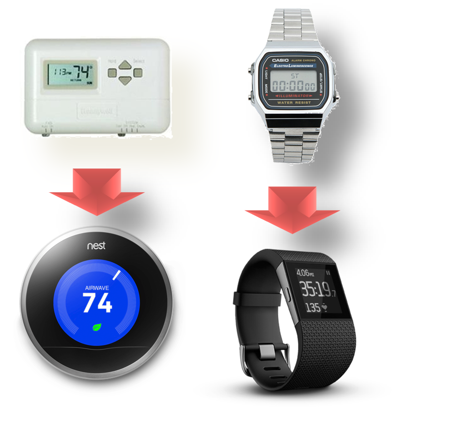
Another interesting change is the increase in complexity of designs targeting a process like 65 nm. If you stand back and think about your own personal life and purchases of products containing electronics, times have certainly changed. Think back say 5-10 years ago—the functionality of the watch, thermostat, or camera you bought is very different from what you expect to purchase today (Fig. 2).
2. Consumer electronics continues the relentless drive toward more functionality and sophistication.
With a growing interest in delivering devices for IoT applications and an overall trend toward “green design,” there’s also a huge push for lower-power devices. The market demand for functionality, speed, connectivity, battery life, etc., within consumer electronics has dramatically increased design complexity.
Today, 65-nm SoCs have more power rails, more power domains, more analog/mixed-signal content, and higher reliability requirements than the first designs based on that technology. Figure 3 gives a good indication of the rise in design complexity, as measured by the number and type of IP blocks in typical designs. One of the implications of these changes—new requirements, more process flexibility and greater design functionality—is a significant increase in the complexity of foundry design rules. This includes added rules for many new device types, and the need to identify design-sensitive yield detractor patterns, voltage-dependent rules, and so on. We refer to this phenomenon as an “advanced mature node.”
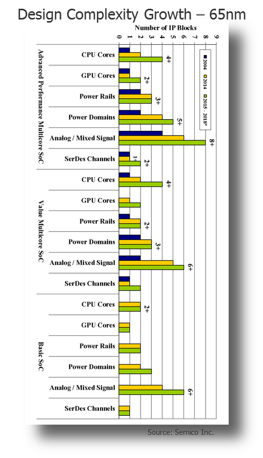
3. Design complexity at established nodes is on the rise—here it’s measured at 65 nm by the number and type of IP blocks in typical designs. (Source: Semico Research)
Why is this important to you? As a reader of Electronic Design, you probably work within the IC ecosystem, developing these types of products using an advanced mature node. Of course, time to market for a new Wi-Fi or Bluetooth chip built on an advanced mature node is just as important as a 16/14-nm application processor for a next-generation smartphone.
Since the design you’re building is far more complex than the first designs built on the target process, your team may be struggling because the EDA tools used when that process was introduced, say 5 or 10 years ago, cannot handle the new requirements and complexity. Fortunately, EDA tools built for later nodes with additional capabilities can be easily redeployed for advanced mature nodes to improve design-team productivity and design quality.
Some of the capabilities commonly employed at advanced mature nodes include:
• Reliability checking to identify design flaws associated with electrostatic-discharge protection, electrical overstress, electromigration, and others in single- or multi-voltage-domain designs.
• Ability to handle voltage-dependent design rules; that is, spacing rules that depend on the voltage potential between devices and wires.
• Ability to check for accurate device symmetry in sensitive analog circuits.
• Pattern-matching functionality to identify specific shapes and configurations that can detract from yield due to lithographic limitations
• Ability to automatically handle DRC waivers so that designers don’t have to track down false errors
• Equation-based design rules, which allow designers to define rules as complex mathematical functions, greatly simplifying rule definition while increasing accuracy.
• An array of other capabilities.
Summary
The latest and greatest IC design and verification challenges are not all at the latest and greatest process node. Competition and market demand continue to challenge designers working at established nodes, too. In addition, industry economics and specialized applications are creating a growing volume demand for designs based on established nodes.
While the market potential of established nodes is growing, so is the complexity and difficulty of validating designs that push these nodes far beyond their original capabilities. The new reality creates challenges for designers using EDA tools that were introduced when the nodes were brand new. We’re learning that EDA tools are not frozen to the node, but must advance at these advanced established nodes just as they do at the leading-edge nodes. Design teams working at advanced established nodes now have the option to upgrade their tools and make their life much easier.

Liked this article? Then try this –

This article was originally published on www.electronicdesign.com
Comments
Leave a Reply
You must be logged in to post a comment.
Yes the eco system being developed for advance node is helping the established node especially in the context of reliability. First pass silicon success for established node has gone up. 28nm node seem to standout at optimum slot at the moment for not so very high-end application. The IoT, consumer electronic legacy designs won’t come down from 65/40, economics wont suit. The NRE for 16nm is way high compare to 28 and above. But high end application with high performance and low power requirement will continue push for 16nm finFET or FDSOI technology.