My Design’s Interconnect Has Enough Wire Width to Withstand ESD… Doesn’t It?
By Frank Feng, Mentor Graphics
Electrostatic discharge can destroy a circuit, but designing adequate protection is not always a matter of blindly adhering to the design rules…

While layout engineers are struggling to implement interconnect that meets chip area goals, they must also be concerned with electrostatic discharge (ESD) design protection on the input/output (I/O) and power/ground (P/G) routing of the wiring. Along the ESD path, the cross-section of electrical current for each interconnection segment (which corresponds primarily to wire width or via area) must be large enough to withstand an ESD surge current.
While interconnect routing is largely automated in physical design, in practice, portions of I/O & P/G routing are frequently performed manually. Designers using a typical routing strategy try to implement wires with enough “total width” for ESD protection when it is necessary to split a wire to connect to a lower level of interconnect layers. To ensure this ESD design practice is followed, the foundry assigns a minimum wire width to meet the ESD requirement (which varies per layer), and a design rule check (DRC) to ensure compliance. Although applying DRC to check for ESD protection has been in use for a while, designers still struggle to perform this check, because a pure DRC approach can’t identify the direction of an electrical current flow, which means the check can’t directly differentiate the width or length of a wire polygon against a current flow (Figure 1).

Figure 1. DRC cannot accurately determine which measurement to use in wire width calculations, because it has no knowledge of current directional flow.
Grouping split wires to obtain an accurate total wire width is also a verification headache, and there is the very fundamental question about what is the “real effective width” or “real effective via area” along the ESD path on each metal segment or via region. Designers learn very quickly that, based on pure DRC checking, the total wire width concept is not a precise measure to ensure their interconnect is safe in the presence of an ESD event.
It is actually current density that is directly correlated to ESD failure, not the wire width by DRC measurement. If the current density along the ESD path on some wire segment or via region is too high, then that wire segment/via region is susceptible to ESD failure. In a simplified static DC model, current density is calculated as distributed electrical current on each wire segment or via area divided by the wire’s cross section (the width of wire segment perpendicular to the electrical current flow) or via area.
Let’s look at an example of why measuring current density, rather than a DRC measurement of wire width, can save a chip design from an ESD crash. Imagine a design team is wiring the I/O path from an I/O pad in the top metal layer to connect to ESD diode/snapback MOS devices in lower metal layers. Due to the foundry limits on device size at each technology node, and the team’s desire to provide enough ESD protection strength, this means implementing many small diode devices (or snapback MOS devices) in an array for ESD protection. However, this approach requires designers to understand the true nature of ESD current distribution on the wired network to ensure their circuits are secure against an ESD event.
Along the as-designed ESD path, wire is routed starting from the higher metal layer connecting to the pad, and then subsequently dropped/stacked down to the lower metal layers to approach the location of the ESD devices. This array of ESD devices also requires an array of lower metal wires to which they can connect. To make this routing connection, at some point (usually starting from some middle level of metal layers) the design must transit from single wiring in one metal layer (Mx) to multiple lines of wiring in the next lower metal layer (Mx-1).
Once the routing splits into multiple wiring, designers typically use a similar pattern of wiring for lower metal layers (Mx-2, Mx-3, …), switching the direction to horizontal/vertical (depending on the preferred direction of assigned routing for each metal layer) when stepping down to connect to the metal1 (M1) wire array. This multiple-lines wiring is designed to meet the designated “total width” for each layer, as defined in the foundry’s design rule manual or technology guidelines. Figure 2 gives you an idea of how the stacked wires look from the higher metal layers to lower metal layers.
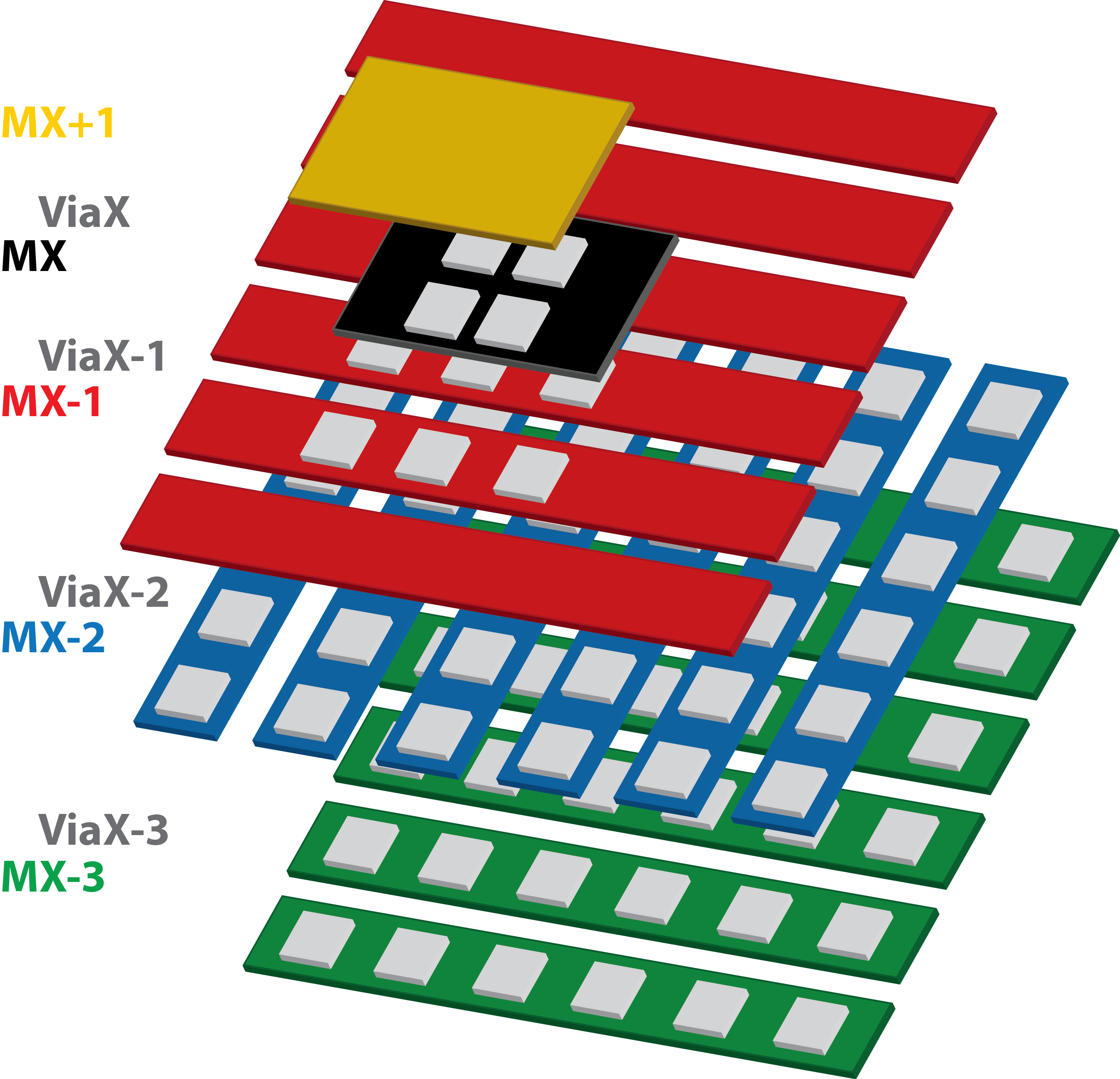
Figure 2. A simplified wire stacking showing routing transits from upper to lower metal layers.
However, a problem can occur in the transition from Mx to Mx-1. The Mx wire (single line wiring) may only overlap, or connect to just a few lines of, the Mx-1 multiple-line wiring. All lines of the Mx-1 wiring (in the form of an array, running in a horizontal direction, e.g.) are well-connected to multiple lines of Mx-2 wiring (also in the form of an array, but running in a vertical direction). When using DRC only to check wire width, all the splitting wire lines of Mx-1 belong to the same node, so the width of each wire is added
up to check against the foundry-defined minimum wire width for withstanding ESD. The routing on the Mx-1 layer passes the DRC checks when all the wire widths are added up.
In reality, however, the effective wire width can’t be simply checked using such a straightforward DRC method. Due to the electrical current flow and distributions in wire segments and via regions of the ESD path, the connection from the Mx wire to the Mx-1 wires causes the electrical current to be distributed mostly on a few wires with or close to VIAx-1 contacts. This uneven distribution means that not all Mx-1 wires shown in Figure 2 are an equal part of effective wire width. The effective wire width can only be calculated by measuring current density, and only simulation can accurately predict current density along each wire segment and via area in the ESD path.
Using a circuit reliability tool like Calibre® PERC™ to perform static DC simulation, designers can use inputs of the resistors network (for example, a SPEF file extracted from a stream-out layout database) and probe points along the ESD path to calculate the current density on each wire segment and via area. With all of these current density measurements, the foundry-defined effective wire width can be converted to a current density constraint to be checked against the simulated current density. In our example, the VIAx-1 and Mx-1 wire segments close to the VIAx-1 area are likely to show a violation, because the current will flow through just the wires close to the vias.
Next time you’re working on a design, don’t let DRC wire width checks mislead you into thinking your layout is safe against ESD. Make sure, using current density checks. Using current density measurements to determine the quality of your protection design can save your chip from an ESD catastrophe.
Author
Frank Feng is a Circuit Verification Methodologist in the Calibre organization at Mentor Graphics in Wilsonville, OR. He is responsible for the development of product functionality to analyze reliability design issues, and to improve the robustness and quality of the design. He also engages with foundries to establish reliability design verification methodology and assist them in converting it into rule kits for designers. Frank holds a Ph.D. in Physics from the University of Houston. You can reach Frank at frank_feng@mentor.com.
This article was originally published in www.semimd.com