Part 1: The 2022 Wilson Research Group Functional Verification Study

In my previous blog, I introduced the 2022 Wilson Research Group Functional Verification Study (click here). The objective of my previous blog was to provide an overview on our large, worldwide industry study. The key findings from this study will be presented in a set of upcoming blogs.
In this blog, I present trends related to various aspects of FPGA design to illustrate growing design complexity.
The Global FPGA Semiconductor Market
The 2021 global semiconductor market was valued at $552.5 billion after experiencing a 24 percent growth over 2020. The FPGA portion of the semiconductor market was valued at about $5.3 billion in 2021. The FPGA semiconductor market is expected to reach a value of $9.3 billion by 2030, growing at a compounded annual growth rate (CAGR) of 6.5 percent during this forecast period. The growth in this market is being driven by new and expanding end-user applications related to data center computing, networking, and storage, as well as communication.
Historically, FPGAs have offered two primary advantages over ASICs. First, due to their low NRE, FPGAs are generally more cost effective than IC/ASICs for lowvolume production. Second, FPGAs’ rapid prototyping capabilities and flexibility can reduce the development schedule since a majority of the verification and validation cycles have traditionally been performed in the lab. More recently, FPGAs offer advantages related to performance for certain accelerated applications by exploiting hardware parallelism (e.g., AI Neural Networks).
The IC/ASIC market in the mid- to late-2000 timeframe underwent growing pains to address increased verification complexity. Similarly, we find today’s FPGA market is being forced to address growing verification complexity. With the increased capacity and capability of today’s complex FPGAs and the emergence of high-performance SoC programmable FPGAs (e.g., Xilinx Zynq® UltraSCALE+, Intel® Stratix®, and Microsemi SmartFusion®), traditional lab-based approaches to FPGA verification and validation are becoming less effective. Later in this blog series, we plan to quantify the ineffectiveness of today’s FPGA verification processes in terms of nontrivial bug escapes into production.
Obviously, both design and verification complexity increase the multiple embedded processes in a single SoC. In our 2022 study we found that 43 percent of FPGA design projects are working on designs that contain two or more embedded processors, while 4 percent of today’s designs include eight or more embedded processors. SoC class designs add a new layer of verification complexity to the verification process that did not exist with traditional non-SoC class designs due to hardware and software interactions, new coherency architectures, and the emergence of complex network on-a-chip interconnect.
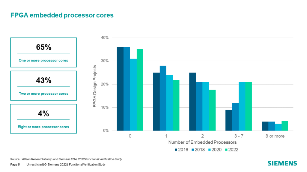
Our 2020 study, for the first time, tracked the number of FPGA projects that have incorporated a RISC-V processor in their design, which was 23 percent, and we didn’t see any significant change in our 2022 study. However, in 2020 we also started tracking the number of FPGA projects that have incorporated some type of AI accelerator processor (e.g., TPU, etc.), which was 19 percent. This grew to 23 percent in 2022.
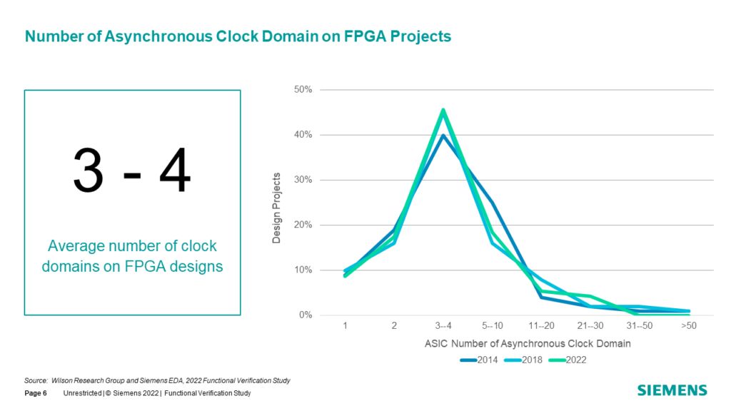
Asynchronous Clock Domains
In Fig. 1-2, we see that 92% of designs being implemented as FPGAs contain two or more asynchronous clock domains. Verifying requirements associated with multiple asynchronous clock domains has increased both the verification workload and complexity. For example, a class of metastability bugs cannot be demonstrated on an RTL model using simulation. To simulate these issues requires a gate-level model with timing, which is often not available until later stages in the design flow. However, static clock-domain crossing (CDC) verification tools have emerged and are being adopted to help identify clock domain issues directly on an RTL model at earlier stages in the design flow.
Security Features
Today we find that 49 percent of FPGA projects add security features to their designs. Examples of security features include security assurance hardware modules (e.g., a security controller) that are designed to safely hold sensitive data, such as encryption keys, digital right management (DRM) keys, passwords, and biometrics reference data. These security features add requirements and complexity to the verification process.
Safety Features
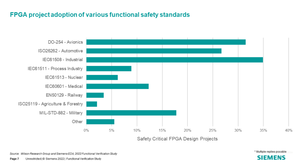
Another example of increasing requirements contributing to complexity relates to safety-critical designs. In 2022 we found that 42 percent of all FPGA projects are working under one of multiple safety-critical development process standards or guidelines.
The key takeaway from this blog is that FPGA designs are growing in complexity, which impacts verification effort and effectiveness.
In my next blog, I’ll focus on verification effectiveness trends related to FPGA designs.
Quick links to the 2022 Wilson Research Group Study results
- Prologue: The 2022 Wilson Research Group Functional Verification Study
- Part 1 – FPGA Design Trends
- Part 2 – FPGA Verification Effectiveness Trends
- Part 3 – FPGA Verification Effort Trends
- Part 4 – FPGA Verification Effort Trends (Continued)
- Part 5 – FPGA Verification Technology Adoption Trends
- Part 6 – FPGA Verification Language and Library Adoption Trends
- Part 7 – IC/ASIC Design Trends
- Part 8 – IC/ASIC Resource Trends
- Part 9 – IC/ASIC Verification Technology Adoption Trends
- Part 10 – IC/ASIC Language and Library Adoption Trends
- Part 11 – IC/ASIC Power Management Trends
- Part 12 – IC/ASIC Verification Results Trends
- Conclusion: The 2022 Wilson Research Group Functional
- Epilogue: The 2022 Wilson Research Group Functional