Part 12: The 2020 Wilson Research Group Functional Verification Study

ASIC/IC Verification Results
This blog is a continuation of a series of blogs related to the 2020 Wilson Research Group Functional Verification Study. In my previous blog I provided data related to designs that actively manage power. In this blog, I present verification results findings in terms of schedules, number of required spins, and classification of functional bugs.
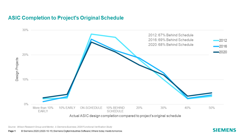
A metric often track to measure efficiency is ASIC/IC project completion compared to the original schedule, as shown in Figure 12-1. Here we found that 68 percent of IC/ASIC projects were behind schedule.
A metric often track to measure effectiveness is number of spins before production. Figure 12-2 presents industry trends from 2012 through 2020 in terms of required spins before ASIC/IC production. Even though designs have increased in complexity during this period, the data suggest that the number of required spins before production has not increased. Nonetheless, only about 32 percent of today’s projects are able to achieve first silicon success.
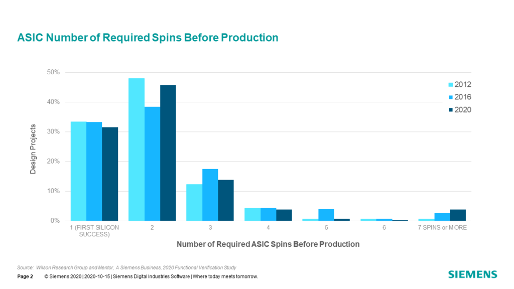
Figure 12-3 shows various categories of design flaws contributing to IC/ASIC respins, where the percentage of “logic or functional flaws” remains the leading cause of bugs. In 2020 we began tracking flaws associated with safety (11 percent) and security (10 percent) features, so we are unable to show trends at this time. Obviously multiple flaws can contribute to bug escapes, which is the reason the total percentage of flaws sums to more than 100 percent.
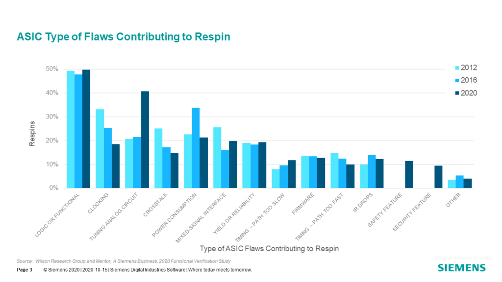
Note that in 2020 we saw a huge increase in flaws attributed to tuning analog circuits (41 percent). I analyzed this year’s results to see whether the spike was restricted to designs at the latest technology nodes, or if it was more widespread. It turns out that while 7nm or below was the most popular answer for those experiencing the problem, it only accounted for about 16% of the cases. Almost all nodes, including 150nm and larger, were seeing these types of failures.
The next thing I looked into was whether these issues existed in only large designs or small ones. The results can be seen in Figure 12-4 below, but it clearly shows that while all design sizes are experiencing a rise in problems associated with analog tuning, the biggest percentage involves the largest designs.
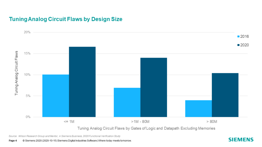
Based on our findings, Semiconductor engineering wrote an article in October on the issue increasing number of analog flaws and interviewed a number of industry experts. One of the key takeaways from this discussion is that we are seeing higher integration of analog across the board in terms of various sized designs, and this is contributing to an increase in analog issues.
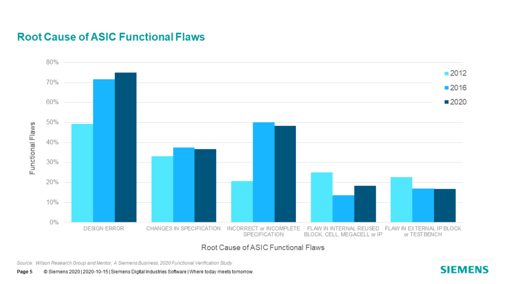
Figure 12-5 demonstrates the root cause of logical or functional flaws by various categories. The data suggest design errors are the leading cause of functional flaws, and the situation is worsening. In addition, problems associated with changing, incorrect, and incomplete specifications are a common theme often voiced by many verification engineers and project managers.
In my next blog I provide some concluding remarks and observations.
Quick links to the 2020 Wilson Research Group Study results
- Prologue: The 2020 Wilson Research Group Functional Verification Study
- Understanding and Minimizing Study Bias (2020 Study)
- Part 1 – FPGA Design Trends
- Part 2 – FPGA Verification Effectiveness Trends
- Part 3 – FPGA Verification Effort Trends
- Part 4 – FPGA Verification Effort Trends (Continued)
- Part 5 – FPGA Verification Technology Adoption Trends
- Part 6 – FPGA Verification Language and Library Adoption Trends
- Part 7 – IC/ASIC Design Trends
- Part 8 – IC/ASIC Resource Trends
- Part 9 – IC/ASIC Verification Technology Adoption Trends
- Part 10 – IC/ASIC Language and Library Adoption Trends
- Part 11 – IC/ASIC Power Management Trends
- Part 12 – IC/ASIC Verification Results Trends
- Conclusion: The 2020 Wilson Research Group Functional
- Epilogue: The 2020 Wilson Research Group Functional Verification Study


Comments