Part 5: The 2012 Wilson Research Group Functional Verification Study
Effort Spent in Verification
This blog is a continuation of a series of blogs that present the highlights from the 2012 Wilson Research Group Functional Verification Study (click here). In my previous blog (click here), I focused on design and verification reuse trends. In this blog, I focus on the controversial topic of the amount of effort spent in verification.
Directly asking study participants how much effort they spend in verification will not work. The reason is that it’s hard to find a paper or article on verification that doesn’t start with the phrase: “Seventy percent of a project’s effort is spent in verification…” In other words, the industry is already biased to respond with this effort value. Yet, there are really no creditable references to quantify this value.
I don’t believe that there is a simple answer to the question, “How much effort was spent on verification in your last project?” In fact, I believe that it is necessary to look at multiple data points derived from multiple questions to truly get a sense of effort spent in verification. And that’s what we did in our functional verification study.
Total Project Time Spent in Verification
To try to assess the effort spent in verification, let’s begin by looking at one data point, which is the total project time spent in verification. Figure 1 shows the trends in total percentage of project time spent in verification for non-FPGA designs by comparing the 2007 Far West Research study (in gray), the 2010 Wilson Research Group study (in blue), and the 2012 Wilson Research Group study (in green).
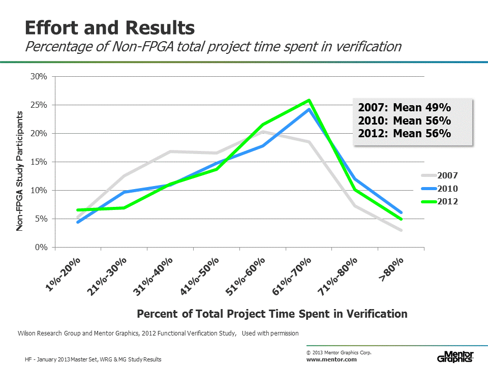
Figure 1. Percentage of total project time spent in verification for Non-FPGA designs
The graph clearly shows that there are some projects that spend a significant percentage of project time in verification (>80%), while other projects spend significantly less time. Notice that in 2007, the average (mean) project time spent in verification was 49 percent, while the average increased to 56 percent in 2010 and remained the same in 2012.
Figure 2 shows the trends in total percentage of project time spent in verification for FPGA designs by comparing the 2010 Wilson Research Group study (in pink) and the 2012 Wilson Research Group study (in red).

Figure 2. Percentage of total project time spent in verification for FPGA designs
You might note that many FPGA projects tend to spend less time in verification than non-FPGA projects. Traditionally, the strategy for FPGA designs has been to get to the lab as soon as possible and debug issues in the lab. In a future blog I’ll show data that indicates this strategy does not necessarily yield good results in terms of meeting project schedule or quality objectives.
Peak Number of Design and Verification Engineers
Next, let’s look at another data point, the average (mean) peak number of engineers involved on a project. Figure 4 compares the growth in recent years for the average peak number of design engineers (in light green) and verification engineers (in dark green) working on a typical non-FPGA project.
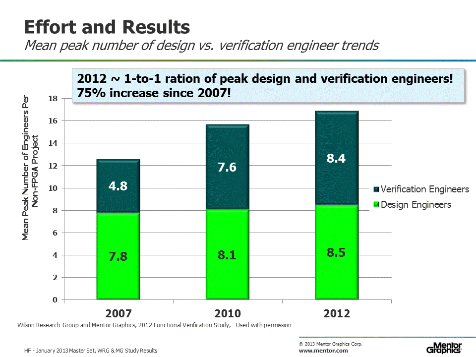
Figure 3. Peak number of design vs. verification engineer trends for non-FPGA projects
Note that there has not been a significant increase in design engineers in the past five years, although design sizes have continued to increase at a Moore’s Law rate. This is partially due to increased adoption of internal and external IP (as I discussed in my previous blog) as well as continued productivity improvements due to automation.
However, the mean peak number of verification engineers working on non-FPGA projects has increased by 75% within the last five years. In fact, today we see (on average) a one-to-one ratio for a project’s peak number of design and verification engineers.
Figure 4 provides a different analysis of the data by partitioning the projects by design sizes, and then calculating the mean peak number of verification engineers by project design. The design size partitions are represented as: less than 5M gates, 5M to 20M gates, and greater than 20M gates.

Figure 4. Mean peak number of verification engineer trends by design size for non-FPGA projects
Figure 5 shows the average (mean) peak number of design engineers (in red) and verification engineers (in pink) working on a typical FPGA project.
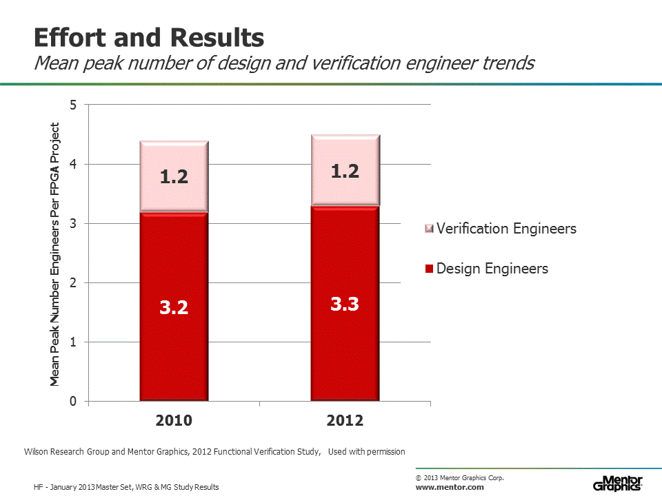
Figure 5. Peak number of design vs. verification engineer trends for non-FPGA projects
Also, note that the ratio of design engineers versus verification engineers hasn’t changed within the last two years for FPGA projects. Typically, design engineers on FPGA projects are responsible for verification too, and you will find many projects that do not have verification engineers. This trend, however, will likely change as FPGA designs become more complex. We are already seeing this on some very complex FPGA projects today.
In my next blog (click here), I’ll continue the discussion on effort spent in verification as revealed by the 2012 Wilson Research Group Functional Verification Study.


Comments