Using EDT Test Points to reduce test time and cost
By Vidya Neerkundar, Mentor Graphics
New EDT Test Points are the next big thing in ATPG test compression

The exponential growth in design sizes has rendered the traditional methods of design-for-test, layout, and timing closure no longer sufficient. Design and test engineers not only have to constantly evaluate new methods and techniques, but they also look for ways to get an edge over the competition through any improvements in the standard techniques that can boost quality or reduce design or test time without undue perturbations to approved design flows. This quest for new and better methods helps the microelectronics industry consistently improve and progress. One new method for scan test that fits the bill as a potential new standard of practice is called “Test Points for embedded deterministic test” (EDT). The use of test points to improve test coverage has been available for a long time, but the new EDT Test Points are unique in their ability to reduce pattern count and hence test time.
For silicon test, several methods are commonly used. In any of the methods, there is some type of automatic test pattern generation (ATPG) compression, or built in self-test (BIST) or hybrid ATPG/BIST engine that is used to target the logic portion of the chip. With BIST, a logic BIST engine that produces random patterns is inserted into each physical region. This logic BIST engine on the chip is turned on to supply the patterns and collect the response of these patterns using a simple test access port.
With scan ATPG compression, which is based on EDT technology, circuitry receives compressed data from the tester, decompresses it within the chip, and then compacts the response for verification. The compression technique helps to reduce test-pattern volume and test time by multiple orders of magnitude. Reducing the test time, while maintaining the same high quality of test, is highly sought after by most designers implementing design-for-test.
Along with the challenges of growing design sizes, designs at newer process nodes present defects that require more than just the traditional stuck-at and at-speed transition patterns to detect. These additional patterns may be targeted towards testing small delay defects, cell-aware defects, etc. In particular, the additional patterns for cell-aware test have had a notable growth in usage for production test. They are essential for designs with very high-quality test requirements. However, these additional pattern requirements increases the pattern count, so new ways to reduce pattern count, improve compression, and reduce test time need to be considered. This is where EDT Test Points come in.
About EDT Test Points
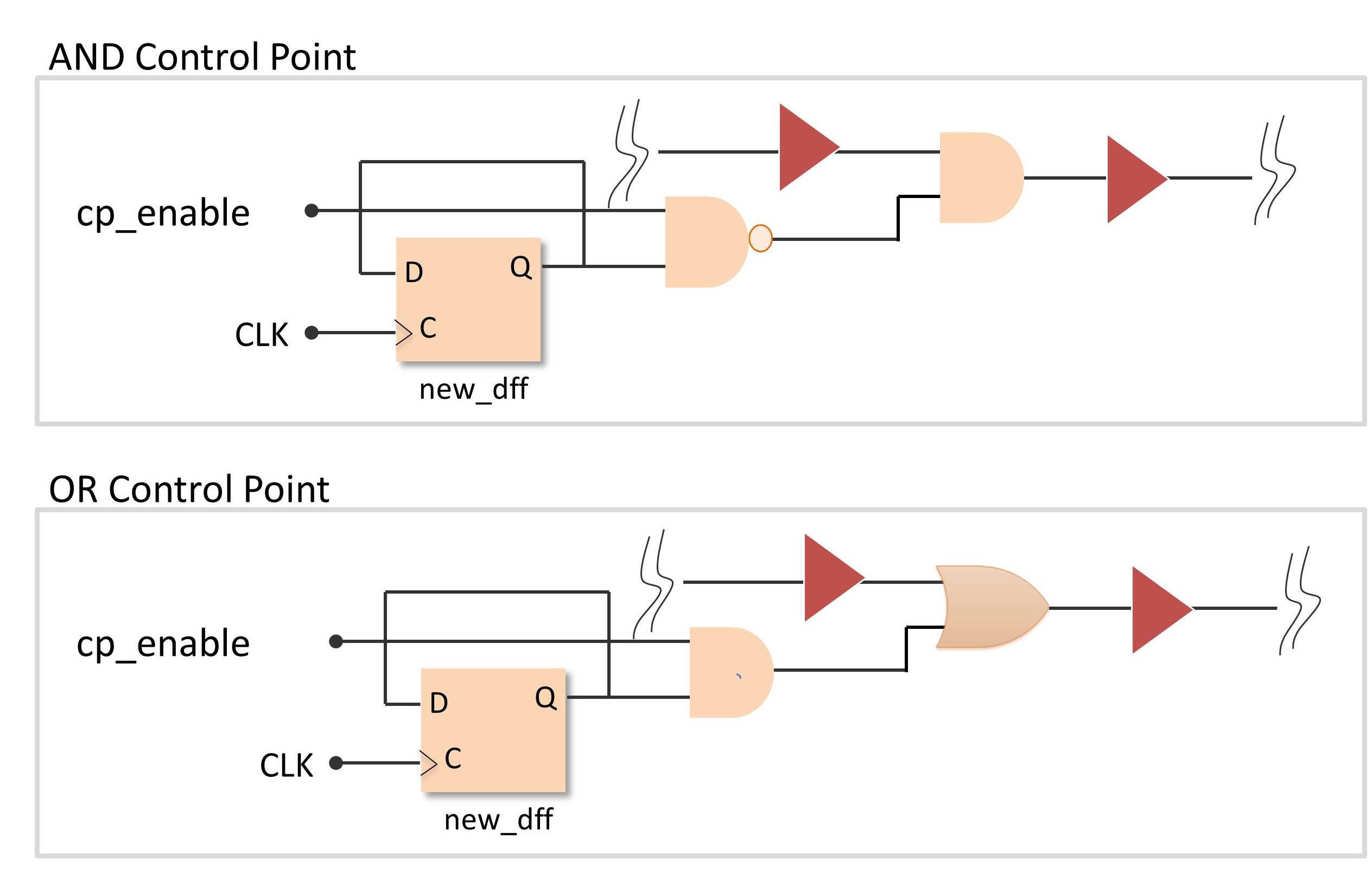
Figure 1. Two types of control Test Point structures. Everything is Test Point logic except for the buffers shown in red.
Traditional test points have been used in the past to improve fault coverage. While they do help improve fault coverage, they do not significantly help improve compression or reduce pattern count. The new EDT Test Points are a unique technology that uses better analysis of where to insert the test points to best reduce pattern count. Figure 1 shows two control Test Point structures. There is an AND-controlled test point and OR-controlled test point. The enable to the control test points can be used to turn off the test points if desired.
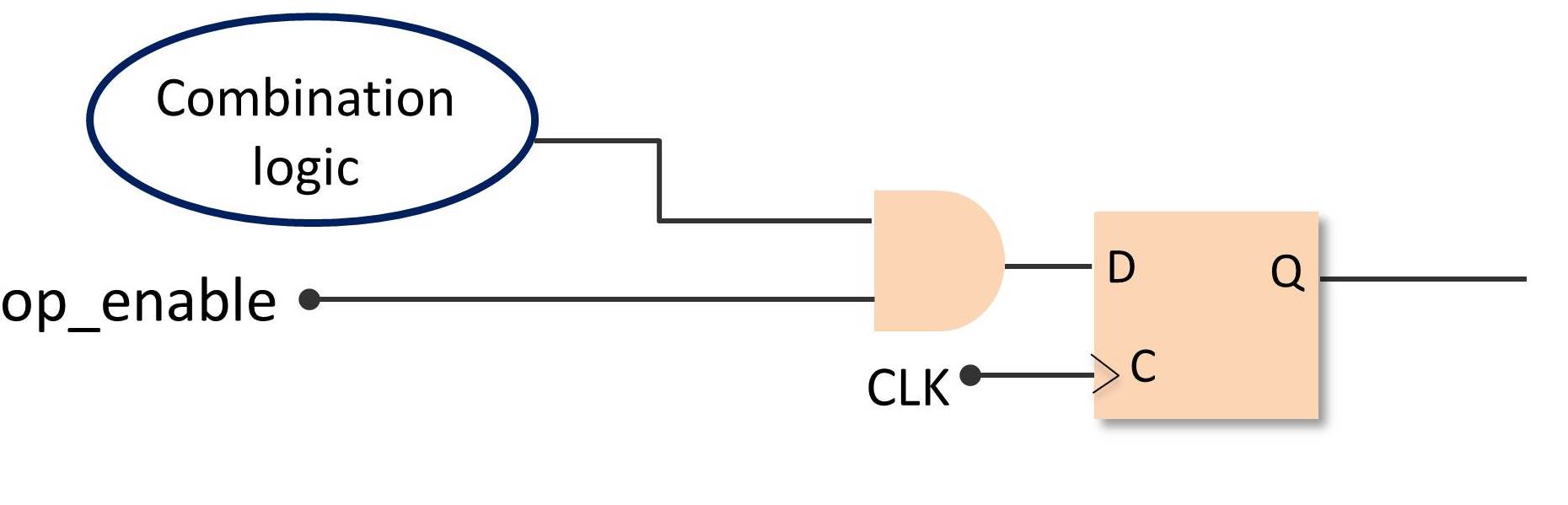
Figure 2. An observe test point structure.
There are also observe-type test points that can be added to improve the observability of specific nodes. Figure 2 shows an observe test point structure. During test point analysis, depending on the nature of the design, the number of control test points and observe test points are automatically optimized. The user, though, retains control over how many of each type and how many total number of test points will be inserted into a given physical region.
The DFT flow with EDT Test Points
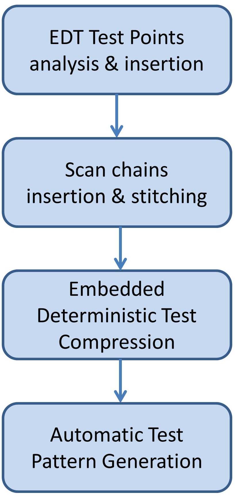
EDT Test Points can be inserted to a gate-level Verilog netlist—either a pre-scan (scan stitching of the flops not present) or a post-scan inserted and stitched design. The flow is described in Figure 3. For a pre-scan design, EDT Test Points are analyzed and inserted into the design, then the scan-chain insertion and stitching (including the EDT Test Point flops) is performed. Next, an EDT compression engine is inserted into the design, and then patterns are generated with ATPG software. For a post-scan inserted design, you specify the starting and ending points of the scan chains that are already stitched during EDT Test Point analysis and insertion. After the EDT Test Points are analyzed, only the test-point flops need to be stitched into scan chains. Then an EDT engine is inserted into the design and patterns are generated.
During EDT Test Point analysis and insertion, false paths and multi-cycle paths can be excluded. Also, modules or instances can be excluded from test-point analysis/insertion. If there are any timing-critical paths they can also be excluded from test-point analysis, so timing closure is not impacted with EDT Test Points. Both observe and control Test Points have their own separate enable, so they can be independently turned on or off during pattern generation if desired. The design before and after test-point analysis can be easily verified formally to be equivalent by disabling the same test point enables.
The number of EDT Test Points a design needs is entirely design specific. Some designs may need less than the average, and some may need more. Typically, 1% to 2% of the total memory elements, including flops and latches, are needed to obtain the desired pattern-count reduction. There is some estimation required, but with any number of EDT Test Points there is a consistent reduction in pattern count. The number of EDT Test Points you insert depends on how much pattern count reduction you want on a physical region.
When EDT Test Points are inserted, they are enabled for all types of pattern that are used to test the design. Table 1 shows the impact of EDT Test Points for two industry designs. The relationship between the number of EDT Test Points and the pattern improvement for both stuck-at and transition (at-speed) patterns are listed. For Design A, with 2% of flops used as EDT Test Points, you see a 1.6X reduction in pattern count for stuck-at patterns and 3.5X reduction in pattern count for at-speed transition patterns. When EDT Test Points are inserted, sometimes there is improvement in test coverage as well, but mostly this is an additional side benefit.
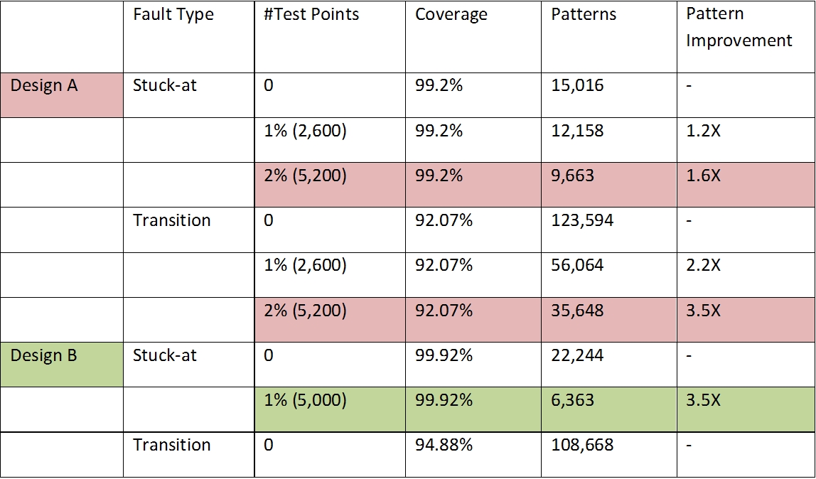
Table 1. Stuck-at and Transition Pattern count comparison for Designs A and B
The use of Cell-Aware patterns has increased very quickly in the past year. However, using cell-aware ATPG results in a 40% larger pattern set than traditional stuck-at and transition pattern sets. To control this increase in patterns, EDT Test Points can be enabled while running Cell-Aware patterns, for both single-cycle and two-cycle Cell-Aware patterns. Table 2 shows the reduction in pattern count for Designs C and E for both single-cycle and two-cycle patterns when EDT Test Points are added. For Design C, with 1.5% of memory elements (flops and latches) used as EDT Test Point flops, there is 1.5X pattern count improvement for single-cycle patterns and 2X for two-cycle patterns. For Design D, there is about 2X pattern count improvement with both single and two-cycle patterns.
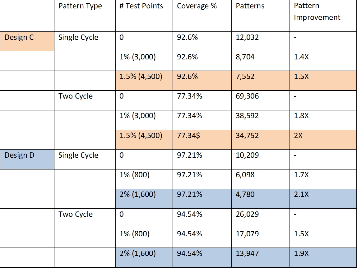
Table 2. Single-cycle, two-cycle Cell-Aware patterns with EDT Test Points
Conclusion
For huge designs at advanced process nodes, design teams need to deploy new solutions to provide quality chips while controlling test time and cost. Any methodology that can be used to reduce test time, contain test costs, and maintain the quality of test is likely to give you the edge over the competition. The value of EDT Test Points is proven through the results we have seen on many industry designs that use them. With the reduction in pattern count achieved with EDT Test Points, you also reduce the time it takes to generate the ATPG patterns and to validate them during simulation. Over all this is a must-use technology for today’s generation of designs.
Author
Vidya_NeerkundarVidya Neerkundar obtained her MS in electrical engineering from Wright State University, Dayton, OH, and now is a technical marketing engineer in the Silicon Test Solutions group at Mentor Graphics Corporation.

Liked this article? Then try this –
White Paper: EDT Test Points
Video: Tessent TestKompress EDT Test Points
This article was originally published on www.evaluationengineering.com