Unlock advanced chiplet design success: Discover the Siemens EDA Heterogeneous Integration eBook series
September 25, 2025
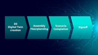
The future of semiconductor innovation is rapidly shifting from monolithic chips to advanced, multi-chiplet architectures. As devices demand greater power,…